Continue to Site

Welcome to EDAboard.com

Welcome to our site! EDAboard.com is an international Electronics Discussion Forum focused on EDA software, circuits, schematics, books, theory, papers, asic, pld, 8051, DSP, Network, RF, Analog Design, PCB, Service Manuals... and a whole lot more! To participate you need to register. Registration is free. Click here to register now.

Op Amp malfunction in SallenKey Filter configuration with Gain

Status
Not open for further replies.
In his first post he said he is multiplexing his RTDs and the unconnected ones cause the opamps to saturate. I think each RTD should be filtered then the outputs of the filters should be multiplexed.

I have never seen an opamp buffer (follower) like from the Microchip application note as shown here. I show three circuits that produce the same output from a low resistance source:
 

Attachments

  • opamp follower.png
    opamp follower.png
    7.9 KB · Views: 110

Hi, I am designing a Data Acquisition System for RTDs, for which i used this application note for analog part. ww1.microchip.com/downloads/en/appnotes/00687c.pdf

I used ADA4004-2 Op Amps instead of MCP609. The application note used 7.47 Gain V/V while i used 8V/V. Moreover, i added another Gain stage(just simple non inverting Gain) after the Filter+Gain stage. The Gain value for next stage is 2.5-5V/V.
Now the issue is that the Op-Amp used in SallenKey+Gain configuration keeps on malfunctioning after some time or is permanently damaged giving saturated value of +15V or -15V. When i replace this OpAmp, new one starts working fine until it faces the fate of the old one.
I would like to add one more thing that i am multiplexing the RTDs and the unconnected ones produce a saturated value at the output, can this be the reason of short life of my OpAmps

- - - Updated - - -

View attachment 116173

This is the image of the Circuit from Application Note

your question is sadly lacking details.
Show your MUX input protection, decoupling and layout.

My guess is the switched voltage transient from cable capacitance of your RTD wires and whatever MUX is damaging the Op Amp.

Vin must never exceed the rails, otherwise latch-up failure may occur.

Similarily as @audioguru pointed out, between +/-15V OA's and 5V ADC
 

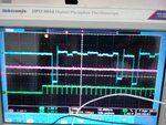
actually the varying input is from the multiplexed channels of RTDs. 16of them. Assume the current be multiplexed. Pots are being used as RTDs, each pot with different value at the moment, each pot is of 500ohm. 1mA sent to each pot where the value of Voltage recieved lies between 100mV to 500mV. The varying Blue signal is the mVolts from the RTDs(Pots). This Blue signal is fed to SallenKey filter Op Amp
 

In his first post he said he is multiplexing his RTDs and the unconnected ones cause the opamps to saturate. I think each RTD should be filtered then the outputs of the filters should be multiplexed.

I have never seen an opamp buffer (follower) like from the Microchip application note as shown here. I show three circuits that produce the same output from a low resistance source:

I believe your analogy is incorrect. The original buffer has a differential gain that cancels wire resistance DC offset and a common mode gain of +1.

- - - Updated - - -

actually the varying input is from the multiplexed channels of RTDs. 16of them. Assume the current be multiplexed. Pots are being used as RTDs, each pot with different value at the moment, each pot is of 500ohm. 1mA sent to each pot where the value of Voltage recieved lies between 100mV to 500mV. The varying Blue signal is the mVolts from the RTDs(Pots). This Blue signal is fed to SallenKey filter Op Amp


The problems are in your layout and design of the mux... MORE DETAILS ARE REQUIRED.
 

your question is sadly lacking details.
Show your MUX input protection, decoupling and layout.

My guess is the switched voltage transient from cable capacitance of your RTD wires and whatever MUX is damaging the Op Amp.

Vin must never exceed the rails, otherwise latch-up failure may occur.

Similarily as @audioguru pointed out, between +/-15V OA's and 5V ADC

The max value AD574 can withhold is 20/10V, i am using it in 10V mode, and in my case, the max Value wont increase 10V, its designed in that way, can this -15V from the difference OpAmp be damaging the SallenKey op amp? i can program my controller to avoid unconnected RTDs.

- - - Updated - - -

I believe your analogy is incorrect. The original buffer has a differential gain that cancels wire resistance DC offset and a common mode gain of +1.

- - - Updated - - -


The problems are in your layout and design of the mux... MORE DETAILS ARE REQUIRED.

Ill upload the detailed schematic very soon
 

Ill share the complete schematic, u may see the above mentioned signals in it
 

At last guys, I performed 100s of experiments on my circuit to get the problem in my hardware but I forgot to review the logic. The issue was that my multiplexed output was switching at almost 40us I.e. 25kHz. While the filter is lowpass with cutoff at 10Hz. Filter was not letting my analog voltage in mV to pass through. Any suggestions what should I do to solve this issue? What kind of noise may effect my RTD mV from the field. Should I go for a bandpass filter or a notch filter? Just to remove the noise that may not effect my signals
 

Filter each signal with its own filter circuit then multiplex the filtered signals.
A shielded audio cable from each RTD will reduce most noise (mains hum and hash from dimmers?) picked up. A notch filter will have no effect on harmonics and hash.
 

I don't believe the multplexing RTDs at 25 kHz serves a purpose. RTD time constants are at least in a ms range. So a reasonable multiplex frequency is most likely in a several Hz up to several 100 Hz range. The filter would still need redimensioning to allow full settling during multiplex time slot.

The selection of suitable multiplex and filter parameters should refer to temperature resultion and expected electrical interferences.
 

Hi,

i already mentionend the filter problem in post#20

and i also mentioned to do the filtering in software (post #11)

this could solve all your problems...


Klaus
 

Ignore specific values intended for high speed MUX. But this is one way to deglitch a MUX.

The LPF is low impedance sample then high impedance hold with low capacitance for fast slew rate during sample and low sag during hold.

Essentially a nonlinear LPF.

adc_guts_sm1.jpg
 

i already mentionend the filter problem in post#20

and i also mentioned to do the filtering in software (post #11)

this could solve all your problems...
Unfortunately the OP didn't manage within six days to post a correct schematic or a problem specification. I fear this is turning out as a helpless case.

It hasn't be clearly specified, but I presume that the intention is to share a single current source and input amplifier for multiple RTDs.
 

Unfortunately the OP didn't manage within six days to post a correct schematic or a problem specification. I fear this is turning out as a helpless case.

It hasn't be clearly specified, but I presume that the intention is to share a single current source and input amplifier for multiple RTDs.

Fist I am really sorry for not uploading the schematic yet, actually i was busy working all possible cases with my circuit and proposing solutions in simulations. Here it is finally , and yes you are right, i want to share my current source and amplification circuitary.

- - - Updated - - -

View attachment ckt.png
All the Op Amps are supplied with +15 n -15Volts

- - - Updated - - -

All the supplies are decoupled with 10nF capacitors too

- - - Updated - - -

Hi,

i already mentionend the filter problem in post#20

and i also mentioned to do the filtering in software (post #11)

this could solve all your problems...


Klaus
I can filter out a predictable high frequency noise with moving average filter, I cant remove 50Hz noise or any other low frequency noise with this kind of filtering in software.

- - - Updated - - -

Please Help me out in choosing appropriate Filter, i removed all the capacitors i.e. removed the filter, shorted the 107k resister, i noticed a ramp wave of 625KHz in the final OpAmp output. This affected the results badly.
 

First point, the multiplexer switch resistance generates a large temperature error when used with the cable resistance compensation circuit. The design idea doesn't work. You'll either disable the compensation circuit (disconnected R5) or use three MUX switches per channel.

Secondly, if you scan the inputs fastly, there's no way to suppress input interferences, e.g. 50 Hz hum.
 

For your first point, I tested this circuit, U3A cancels the 4ohm Mux resistance, or i can fix this in my software. Can there be any solution if i reduce my switching speed to 25Hz, i tried doing it but any LPF can allow 25 and stop 50Hz. specially when 25Hz is in this shape
2.jpg
 

Yes. You need to maintain continuous current for each RTD perhaps using current mirrors.

Recall V=L di/dt

or slow down and control di/dt with OVP added.
 

My current is already very clean but FIeld environment is very noisy, I am using very precise Regulator to generate 2.5V for CUrrent, and my supplies are from EMI filtered DC DCs
 

Hi,

it seems your sampling frequency is about 32kHz. if not, please tell us your sampling freuency.

if you now continously sample 32 input channels, then you get a sampling frequency of about 1kHz per channel.

If this is true, then for sure you can filter out low frequency (like mains frequency) in software. ...

Noise / frequency up to 500Hz (theoretically) can be filtered out.
Problematic are unpredictable frequencies above 500Hz. These cause alias frequencies, that not can be filtered out with software.
But also for this case there are techniqes to suppress those frequencies.

In my eyes filtering of mains frequency on the analog side, and on the other side selecting channels with 32kHz is impossible. They fight each other.

Btw filtering before the ADC: If you just use a simple RC as filter and want your ADC to sample with a precision of 0.1% then you need to wait at least 7 x R x C.
"Wait" means you should select the channel and then you need to wait 7RC before you start to convert the signal.
If you don´t wait you will see a crosstolk of the channel before.
Calculation: if your sample rate is 32kHz this means you have about 30us for each channel. Maybe converting needs 10us then you have about 20us for the signal to settle.
20 us are 7RC. so RC is about 3us. In other words: your RC filter needs a cutoff frequency of more than 53kHz.

**
The key is to use independent software filters for each channel. While this is possible in software it is not with your single external analog filter.
So with software you need a biquad for each channel and within one biquad you process data of only the corresponding channel.
The the biquad only sees the ADC data of one channel and therefore it is not influenced by the voltage of the other channels.
(it does not know that the inputs are multiplexed)

Instead of biquad you also could use IIR filtereng. Even averaging is possible. But mind to average every channel independently.

*********
Your MUX: as mentioned by FvM the resistance of the MUX causes errors. They mainly depend on switching voltage, supply voltage and temperature.
Splitting your signals to/from the RTDs in "force" and "sense" channels (kelvin matrix) may solve this problem. But at least one extra 1:32 MUX is necessary.

****


Klaus
 
  • Like
Reactions: fouwad

    fouwad

    Points: 2
    Helpful Answer Positive Rating
I missed your post of a schematic in #34. { oh shame on me}

The problem is clear to me now that input impedance is very imbalanced and floating in the special cct U3A.

The intent is to provide non-inverting unity differential gain which cancels common mode voltage drop on cables when the sensor is low impedance and voltage drop on cables can be significant.


Unfortunately the input impedance is unbalanced.

If you resolve your very high input impedance to stray current or voltage during switching, then your performance and reliability will improve and include transient suppression as required.


EMC analysis can be tricky. But imbalanced high impedance lines are a major cause of susceptibility and switched imbalanced lines even worse.

in conclusion a shielded single current loop is farily immune with CM Choke for RF but a switched current loop is cause for concern with a floating input.
 

Status
Not open for further replies.

Part and Inventory Search

Welcome to EDABoard.com

Sponsor

Back
Top