Continue to Site

Welcome to EDAboard.com

Welcome to our site! EDAboard.com is an international Electronics Discussion Forum focused on EDA software, circuits, schematics, books, theory, papers, asic, pld, 8051, DSP, Network, RF, Analog Design, PCB, Service Manuals... and a whole lot more! To participate you need to register. Registration is free. Click here to register now.

Offline flyback SMPS needs conformal coat over via?

cupoftea

Advanced Member level 6
Joined
Jun 13, 2021
Messages
3,072
Helped
62
Reputation
124
Reaction score
139
Trophy points
63
Visit site
Activity points
16,044
Hi,.
We are hipot testing an offline flyback PCB. The flyback is totally enclosed in
an earthed metal enclosure.
Unfortunately, on the secondary side, there is a via under a connector, and this via is
just 1.2mm away from a bit of the earthed enclosure. As such, this flashes over
and causes hipot fail, since the actual earth must not be connected for the hipot test.

Anyway, i spread some acrylic conformal coat over the via and left it to cure.
But when it had cured, the conformal coat had parted itself away from the via, and so the via
is still exposed, even though i pasted conformal coat right over it. As such, the board still fails flash test.
Do you have any ideas for ways in which i can get the conformal coat to cure and stay
covering the via? The via is just 0.3mm hole and 0.6mm diameter (round). We cant drill the via out as this would expose internal
ground plane and we would then just fail hipot on that.
 
BTW when testing L&N from PE gnd, the floating case is not null when Y caps are balanced but 50% of the input line transient.

There is no need to connect secondary to the generator. If you connect secondary 0V to PE ground to case, is almost the same thing except now if your case is floating at nearly 50% of the input. (so your method is valid in testing this way assuming installation errors)

A 50 Hz 2-second burst is a thousand times less stressful than a 1us pulse with 1us risetime. Remember that Ic=CdV/dt, and human touch impedance is mostly capacitive.

The best solution is a Balun on the input which now acts as a differential LC filter with L&N shorted and then a CM filter for the flyback noise when operational.

I wonder why a 2s 50Hz burst at 4kVrms was used. hmm.
 
Last edited:
A 50 Hz 2-second burst is a thousand times less stressful than a 1us pulse with 1us risetime.
Thanks, yes i see your point, these transients are said to be very fast...but i dont see how such spikes get through all the stray L's in front of them in the mains supply grid......and how could such a thing raise up the voltage on the post_Boost_PFC caps. (or post FWB cap).

Mains transients are so weird...nobody has ever caught one of them on an oscilloscope.
 
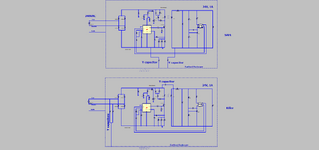
Basically the crux of the matter is the following...

..The two shown isolated offline flybacks are identical. -Apart from the Y capacitor positions.

The top one is safe, the bottom one would kill you if you touched the metal earthed enclosure
and the enclosure had mistakenly not been earth connected when the product was assembled.
(pri and sec tracks are each 3mm away from the metal earthed enclosure, and 6mm apart from each other)

Since Y capacitors are so life/death crucial, why do we not have "y capacitor inspectors" taking apart
SMPS to see how the Y caps have been done?
 

Attachments

  • Y caps in isolated SMPS.png
    Y caps in isolated SMPS.png
    52.8 KB · Views: 42
Yes. 1nF (or so).
Remember that this concerns those "bad" units which got out of production without the chassis being connected to earth..
(the standards say we must give full consideration to this)
If we look at the equivalent circuits....the top one has the chassis as the mid point of a 1n/1n capacitive divider between pri and sec.
The bottom one will end up with the full pri-sec voltage between sec and chassis....and there is only 3mm clearance between them....
Unfortunately, a deadly situation for someone touching the chassis. Tragically, a death certificate is likely for someone.
 
Hi,

1nF @ 50Hz is about 3MOhms.
The current at 230V AC is limited to 72uA. Not enough to kill.

Indeed the purpose of these 1nF capacitors is to
* give the high frequencies a path to reduce EMI
* still limit an erroneous current at mains frequency to a non dangerous value.


Klaus
 
Thanks, but mains transients, ayk, are 10us rise time, the equivalent frequency is very high....so Y cap Z is very low....if you touch chassis at the instant
of the transient, then one dies. The standards are big on this.
 
Hi,

but those Y-capacitors are not at the HF switching node. This would not be allowed!
They are at the mains frequency nodes. Also at your schematics.

So what 10ns rise time transients are you speaking about?
* Either they are of lower voltage -->not dangerous
* or they are rare --> to low energy to be dangerous

And they are not normal 10nF capacitors. They are Y rated. This means they are designed to fail OPEN ... not to cause a path for dangerous currents.
And they are designed for high voltage peaks without getting damaged at all.

Klaus
 
Yes, there is a risk. That´s why series inductors are useful.
Thanks, i agree, but there is no stipulation in the standards for inductors to quash mains transients. The bottom schem (as shown above in post #23 )
will fail hipot test at 4kv rms...since the 3mm will flash over with 4kv rms test voltage across it.

This fail is ultimately due to the fact that its life-threateningly dangerous (the bottom one).
The standards declare it thus.

Just that little difference in Y capacitor positions means the difference between life and death.
 
I think most of your considerations is wrong or inappropriate. Although you are confusing test and working voltage, even 4 kV doesn't flash over 3 mm clearance. Required clearance for 230 V mains, overvoltage category I (equipment connected to regular wall outlets) and reinforced insulation is 1.6 mm according to safety standards.
 
even 4 kV doesn't flash over 3 mm clearance.
Thanks, but i have actually done this many many times with the bottom schem of post #23 above...and with 3mm of clearance between pri and chassis, and between sec and chassis, and it definetely does flash over with 4kv rms.
(There was of course, the regulatory 6mm of clearance between pri and sec).

The fact is that the bottom schem of post #23 is a killer, and fails the 4kV flash test...the top one, even though only very slightly different , (by way of Y cap position) is perfectly safe, as per it doesnt flash over with 4kv rms applied between pri and sec. So the standards say its safe.
This is a great example how a single Y capacitor connected between secondary and chassis can save someone's life........or sadly take someone's life if it is not used, or goes open circuit.

Please remember we are talking about the chassis mistakenly NOT getting connected to earth whilst in production....that is when the life threatening danger occurs...and the standards tell that it must be taken account of.

Obviously if the chassis is connected to earth, then no one will die when touching it.....but the standards say (and rightly so) that we must consider when the chassis mistakenly doesnt get connected to earth....and thats when the bottom schem of #23 above, will kill us.

There is also the situation of equipment installed on land that is very dry and non conductive, eg clay etc......because then even earthing the chassis will still bring problems if a person touches it.

So yes, its literally a 1nF Y capacitor standing between life and death !

Believe me i have tryed to look at this from other ways...i mean, we have a customer who has 200 PCBs made up like the bottom schem of post #23 above...and they want us to either modify them to be like the top schem of post #23, or find "some other way around it".
They have 3mm of clearance between pri and chassis, and 3mm clearance between sec and chassis, and 6mm between pri and sec.....and i can gaurantee, the bottom one of post #23 (above) flashes over with 4kv applied pri-sec (when chassis is floating, ie, not connected to earth)

I keep thinking "this is madness"....but when you look deep down and logically at it...its true...literally a Y 1nF capacitor stands between life and death!

It would be good, and please may i ask, if this part of this thread could be hived off into a new post at all?, titled...."Y capacitor is difference between life and death in offline SMPS?"....since it is not going to be recognised being buried in this thread , as such. -My apologies for that...the original problem at first seemed different to the actual problem that it is.
 
Last edited:
Hi,

3mm clearance to metal enclosure in offline , isolated SMPS...
Imagine you have an offline, isolated SMPS in a metal case.
Y caps connect incoming Line and Neutral to the metal case.
There are no Y caps connecting secondary side to metal case.
The secondary side circuitry is all kept more than 3mm away from the metal case.
-But some secondary tracks are actually just 3mm away from the metal case.

The primary side circuitry is all kept more than 3mm away from the metal case.
-But some primary tracks are actually just 3mm away from the metal case.

During assembly , someone forgets to connect the metal case to the incoming earth wire in the mains input cable.

Is it ever going to be dangerous for someone to touch this metal case? (remembering that it has mistakenly not been attached to earth)

Also, supposing there is comms and signal processing circuitry at the secondary
side of the SMPS. Do you think that the fact of the earthed enclosure not being actually connected
to earth could result in problems for the communications equipment?
 
Last edited:

LaTeX Commands Quick-Menu:

Similar threads

Part and Inventory Search

Welcome to EDABoard.com

Sponsor

Back
Top