Continue to Site

Welcome to EDAboard.com

Welcome to our site! EDAboard.com is an international Electronics Discussion Forum focused on EDA software, circuits, schematics, books, theory, papers, asic, pld, 8051, DSP, Network, RF, Analog Design, PCB, Service Manuals... and a whole lot more! To participate you need to register. Registration is free. Click here to register now.

Offline flyback failing HiPot test.

cupoftea

Advanced Member level 5
Joined
Jun 13, 2021
Messages
2,930
Helped
59
Reputation
118
Reaction score
134
Trophy points
63
Activity points
15,519
Hi,
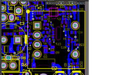
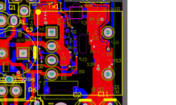
We have an offline , isolated 24W Flyback in an earthed
metal enclosure.
We use TO220 Plastic FET in primary and TO220 plastic
diode at secondary. They are both screwed to the same metal heatsink.
(with no insulation pad)
Then when we apply our 4kVrms (between L+N and output for 2 seconds, it is failing.
Do you believe we need an insulation pad?

When i say its failing, it doesnt indicate failure, but we can hear fizzling at 4kV indicative of breakdown.
The 0-3mA current meter reads no current.
 
if capacitance to floating conductor is higher than conductor to air the conductor will charge up. C is proportional to area/gap
Thanks, i thought it must be something to do with stray C's.
So if the C from Floating_copper to nearest_track is greater than the C from floating_copper to "xxxxxxxx", then the floating copper will charge up.
....Please may you advise what is "xxxxxxx" above?

I suspect any floating copper on the PCB will (albeit slowly) charge up to the highest hipot voltage, ie 4kv * sqrt(2) = 5650V. Am i correct?....or less if it flashes over to something in its vicinity. (which incidentally, means the unit fails due to breakover).
Also, we have many SOT23 diodes on our PCB, each of which, of course, have a "third pad" which cannot be
connected to anything (ie, it must
float). What do we do about these? They will surely be induced up to 5.6kv (during hipot test) and then flash
over to the adjacent pads on the
same footprint?
 
Last edited:
The relative C of every path depends on area/gap * Dk for gap to ground for a simple 2D model.
Diode C is max at >=0Vf.
xxx absolute = don't care for now.

C*V=Q will be constant in each dielectric between floating conductors if the small leakage current is constant (rms)
So the largest V drop is across the smallest C in a series loop to ground.

There may be many parallel paths to ground and each is independent for Q=CV with the minimum gap, x and V/x is the E-field and Dk scales up C vs air =1.

Contaminants (e.g. flux & dust) lower creepage resistance.

If you want to look for PD or corona or e-field use a Big R current limited Vac to find trip threshold.
You can also do a slow ramp with DC.
 
It would be interesting if OP could upload a video clearly showing the monitor distortion happening with the PSFB on no load...then showing the monitor distortion being relieved when OP loads up the PSFB....but i very much doubt that such could even ever happen.

There is an issue with PSFB, that it can be somewhat inefficient in light load when in its simplest form....i think and suspect that this is what the OP is trying to get into(?), and is picking the no_load case "ringing" as a target to go for, for investigation, in order to try and do something about the light load inefficiency of PSFB...am i right?
--- Updated ---

Hi,
Back on the offline flyback that's failing 4kv hipot test if I may.. The transformer is shown in the attached 2 pics of the layout.
The transformer is E25/13/7. Its wound pri/aux/sec = 84/14/19 (no sandwich).
The pri is the first coil on the bobbin. The pri is the only coil that's enamelled copper wire. The
aux and sec are TIW.
As you can see, there are a number of SMD components with sharp cornered edges right under the transformer.
(well, on the bottom , blue layer)
I wonder if these are flashing across the isolation barrier via the transformer? The PCB is 1.6mm thick and
just the 2 layers , top and bot.
The transformer is only spec'd 1kv from P-S to core.

The other pic shows the red top layer aswell...its copper pours.
 

Attachments

  • ___Flyback transformer hipot_bottom components.png
    ___Flyback transformer hipot_bottom components.png
    205.6 KB · Views: 28
  • ___Flyback transformer hipot_with top copper pour.png
    ___Flyback transformer hipot_with top copper pour.png
    199.5 KB · Views: 28
Last edited:
Qu 5: Hipot testers produce overly high voltage due to Y capacitors?
Hi, We had an offline flyback fail 4kv hipot testing from L+N to output.
The flyback is in an earthed metal enclosure.
Obviously the metal enclosure is not earthed for the hipot test, as that is against the regulations.
(the earthed enclosure, which is screw connected to the PCB copper, is obviously floating for the
hipot test. And of course, it can act as a conduit for flashovers from pri to sec.)
The flyback has a Y1 cap across the transformer (pri to sec). It also has a Y2 cap from earth screw
to HVDC+(pri).
We taped up all the places where the breakover could be happening, but the breakover then continued to be
seen.
So the contractor has now told us to repeat the test with the two Y caps removed.
Why would he say this?
Is it because, as EasyPeasy implied, that Hipot testers can go "haywire" when they operate
into y caps and then they can produce far higher peak voltages than they should do? (and thence
we are seeing the flashover?)

*Qu 6: PCB Inner Layer Creepage distance from primary to secondary circuits?
Hi, with this Hipot_failing two layer flyback design, we reckon we can get more separation from
primary to secondary by going to a 4 layer PCB. For primary to secondary creepage distances
in a PCB inner layer,
do you know what is the allowed minimum distance?, ie, are they the same as for external layers?
 
Last edited:
Qu 7: Failing hipot due to metal enclosure.
Regarding the offline flyback (in earthed metal enclosure) which is failing 4kv hipot test
from pri to sec. Obviously the earthed metal casing and PCB screw etc is all just floating for the test,
as required by the standards.
As can be seen from the attached, the mains input connector is phoenix 1726040

Phoenix 1726040 MAINS CONNECTOR.

The problem is as seen on page 7 of the connector datasheet (above).
The metal pin comes up along the back of the connector and is very close to the back of the connector. In the layout, this back of
this connector is right up against the metal enclosure wall. The capacitors C5 and C11 are also right up against this
same metal enclosure. So this is why we are seeing so much flashover. We are putting transformer tape over the enclosure
next to the capacitors...but it makes no difference....because the flashover just tracks right along the tape and goes round it,
as if the tape isn't even there.
Would you agree that we will never get this PCB through this hipot test until we are able to move the said
proponents away from the metal case?
 

Attachments

  • PCB hipot fail via mains connector.png
    PCB hipot fail via mains connector.png
    151.5 KB · Views: 33
If I could hear corona discharge/arcing, but the hipot current measurement indicates "zero current", then I would immediately assume my test equipment is faulty or set up improperly. Solving that mystery comes before trying to determine the cause of the arcing.
 
If I could hear corona discharge/arcing, but the hipot current measurement indicates "zero current", then I would immediately assume my test equipment is faulty or set up improperly. Solving that mystery comes before trying to determine the cause of the arcing.
Is this a CM line test to PE ground? Both arcing and null current must be resolved by route cause analysis.
 
If I could hear corona discharge/arcing, but the hipot current measurement indicates "zero current", then I would immediately assume my test equipment is faulty or set up improperly. Solving that mystery comes before trying to determine the cause of the arcing.
Thanks, its not zero current , but below 1mA.
To be honest, would you expect the arcing currents (the audible cracking and fizzling) ...which are probably 50us long and occur in bursts...possibly at T = 10ms or so.....and as such, i wouldnt expect the current meter to register it?

Is this a CM line test to PE ground? Both arcing and null current must be resolved by route cause analysis.
Thanks..this is L+N to output.

The PCB of this post is only prototype, never seen the proper light of day, but any answers to the above multiple questions much appreciated.?
--- Updated ---


Last sentence of this says hipot testing can damage equipment...
https://tomdunnacademy.org/hipot-testing-101/
"Excessive voltage levels or extended test durations can increase the risk of insulation breakdown, equipment damage, or electrical accidents."
 
Last edited:
Normal Hipot is always L&N to nearest ground not output. but if an isolated DC is PE grounded then the testing is like L&N to Output with big shunt caps.

Otherwise never to an isolated output unless you trying to test for redundant isolation by bypassing your trafo.

My Hipot testers had analog 0 to 100 uA meters.

If you had 20 mA arcs for 50us every 10 ms then the duty factor d.f. = 5/1000 thus I avg=5*20mA/1000 = 100 uA.
 
If you had 20 mA arcs for 50us every 10 ms then the duty factor d.f. = 5/1000 thus I avg=5*20mA/1000 = 100 uA.
Thanks, i am not sure if a cheap current meter (possibly such as on the hipot tester) would be able to average it out?
But yes, youre right, thats about what current we are seeing...a few 100 uA's, so maybe it did average it out, who knows.

Normal Hipot is always L&N to nearest ground not output.
Thanks, with offline SMPS, i beleive hipot is always done (L+N) to isolated output (+_-), whether or not earthed sec.
 
Thanks, its not zero current , but below 1mA.
To be honest, would you expect the arcing currents (the audible cracking and fizzling) ...which are probably 50us long and occur in bursts...possibly at T = 10ms or so.....and as such, i wouldnt expect the current meter to register it?
The current measurements in a hipot measurement can actually be quite sophisticated. Last time I worked on a hipost test, I was using a GW Instek 9603, which has an RMS current measurement (presumably similar to how a DMM ammeter works) and also "arc detect" which designed specifically at catching high frequency content (but how this works is not clearly defined). IIRC the instrument did not really display the measured "arc" current.

Whether the arcing should constitute a failure in your test depends on the particular standard you're applying (for type testing) and your own risk analysis (for unit testing).

This link gives a good overview of arc detection: https://www.ikonixusa.com/whitepapers/the-truth-about-arc-detection
--- Updated ---

Normal Hipot is always L&N to nearest ground not output. but if an isolated DC is PE grounded then the testing is like L&N to Output with big shunt caps.
I'm guessing by "output" he means secondary side, not necessarily the + output terminal. But if the secondary is not referenced to PE, I suppose either output terminal could be used....

IME most of these rules of thumb about how to carry out these tests depend on whether a single device/psu is being tested, or whether it's a test of an assembled device including a PSU.
 
Last edited:

LaTeX Commands Quick-Menu:

Part and Inventory Search

Welcome to EDABoard.com

Sponsor

Back
Top