Continue to Site

Welcome to EDAboard.com

Welcome to our site! EDAboard.com is an international Electronics Discussion Forum focused on EDA software, circuits, schematics, books, theory, papers, asic, pld, 8051, DSP, Network, RF, Analog Design, PCB, Service Manuals... and a whole lot more! To participate you need to register. Registration is free. Click here to register now.

LVS problem: Parasitic NW to P-sub junction diode is not formed

Minh_Hoang_Le

Newbie
Newbie level 3
Joined
Oct 13, 2024
Messages
3
Helped
0
Reputation
0
Reaction score
0
Trophy points
1
Activity points
23
Dear all,

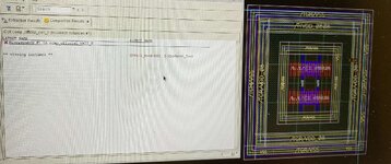
I am designing an Op Amp on 22 nm FDSOI process and having a problem on the layout of the PMOS pair.

I use the super-low vt tripple-well PMOS device for my PMOS pair (flip-well PMOS device). The pair is broken down into several sub-cells for layout matching pattern ABBAABBA. I have already built 3 guard-rings for the whole matching structure, which includes one inner PWGR connected to VDD, one middle DeepNWGR connected to VDD, and one outer SUBGR connected to VSS. However, when running LVS, calibre tool still says that my layout does not have the parasitic NW to psub junction diode. I think the outer SUBGR connected to VSS and the middle DeepNWGR connected to VDD should form this parasitic diode, but no at all.

Anyone has any idea on this problem?

Thank you!
 
Last edited:
Hi @Minh_Hoang_Le
I think that the problem might be in your triple-well structure.
Could you please explain what is the need to use of triple-well structure for PMOS devices? It doesn't make any sense for me and I haven't seen anyone doing this. Usually, for PMOS it should be an NWELL only.
 
Hi @Minh_Hoang_Le
I think that the problem might be in your triple-well structure.
Could you please explain what is the need to use of triple-well structure for PMOS devices? It doesn't make any sense for me and I haven't seen anyone doing this. Usually, for PMOS it should be an NWELL only.
I use the tripple well device because I negatively bias the body of the PMOS device, which is a feature of FD-SOI technology. This is a 6-terminal device. If you use the same technology like me, I think you can see the cross-section structure of the flip-well PMOS device for negative bias, which is a normal PMOS low-vt device including 3 parasitic diodes - one from P-well to Deep N-well, one from P-SUB to Deep N-well, and one from normal NW to P-SUB.
 
Calibre says that the parasitic diode is missing, so there is no highlighted area. The weird thing is that I break the PMOS pair into 8 devices in total, only the PMOS_4 on the right hand side is reported on this problem. I try to bias the inner guard-ring with both VDD and VSS, but this problem still stays there.
 

Attachments

  • 462270687_1273141507452813_5174930311847282789_n.jpg
    462270687_1273141507452813_5174930311847282789_n.jpg
    219.6 KB · Views: 11
FDSOI is necessarily a very thin film and the "deep" features you mentioned are impractical to make.

Deep N well would normally be a couple of microns and FDSOI film thickness has to be less than 900nm (by my experience, at this point intrinsic FETs will deplete fully, here, at Vgs=0, but logic-VT FETs will not - "real" modern FDSOI runs thinner).

I think you are applying rules from some other branch, or if a root flow includes both triple well and SOI branches maybe a switch setting or an invocation of an altogether different deck.

Note that while SOI improves isolation the "vertical curtailment" may well put some library elements out of reach - like any that need that Z axis depletion spread to block high voltage. I see this on one flow that I've worked both sides of - JI will give you HV diodes and LDMOS, SOI variant has nothing over 6V.
 
Last edited:

LaTeX Commands Quick-Menu:

Part and Inventory Search

Welcome to EDABoard.com

Sponsor

Back
Top