Continue to Site

Welcome to EDAboard.com

Welcome to our site! EDAboard.com is an international Electronics Discussion Forum focused on EDA software, circuits, schematics, books, theory, papers, asic, pld, 8051, DSP, Network, RF, Analog Design, PCB, Service Manuals... and a whole lot more! To participate you need to register. Registration is free. Click here to register now.

Loop Gain Stability - LTSpice

Status
Not open for further replies.

Smillsey

Member level 5
Member level 5
Joined
Jul 7, 2014
Messages
91
Helped
0
Reputation
0
Reaction score
1
Trophy points
1,288
Activity points
2,121
Hello all

I am having problems tracking down the problem with a current source circuit, so I thought I would plot the loop gain and check the gain/phase margins.

I thought I would first go back to basics and used a guide I found on youtube to plot the loop gain. I am not sure exactly why this method works (using split sources (V1 and V2) and a dependent voltage source (B1), but it does work well and I would rather concentrate my efforts upon understanding the problems with my circuit.

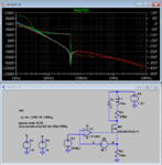
I have attached "loopgain1.asc" which is a test circuit to check the that loop gain measurement method works, I am happy with this test and if you plot the following graph you see the loop gain of the follower circuit;

(I(V2)@1+I(V1)@2)/(I(V1)@1+I(V2)@2)
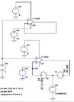
loop_gain_test_circuit.JPG

graph_formula.JPG

loop_gain_gain_margin.JPG

loop_gain_phase_margin.JPG

With a gain margin of 25dB and phase margin of 54 degrees, this circuit is stable.

In my next post I will post up my current source, this may take a few posts - I am sorry about that!

Thanks.

- - - Updated - - -

To help any future readers of this thread, I thought I would post a plot of the effects of a capacitive load, in this case 1uF.

For clarity, the first plot is without the 1uF load and shows no oscillation;

resistive_load_stable.JPG

With the 1uF load added, we get into problems;
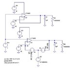
loop_gain_capacitive_load_circuit.JPG

capacitive_load_step_response.JPG

The reason? Interaction between the output impedance of the op amp (known as Ro) and the capacitive load, which gives rise to another pole in the loop response, this destroys the gain margin we previously had. The loop gain plot now shows +21dB @ 180deg phase shift, this is positive feedback and we have ourselves an oscillator.

capacitive_load_gain_margin.JPG

Next, I will introduce the current source.

- - - Updated - - -

Here is a very basic (with no compensation) current source, it is unstable.
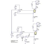
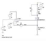
current_source_loop_gain_circuit.JPG

So I perform the same loop gain test, linking the dependent voltage source to be the same voltage at node Vfb

current_source_loop_gain_gain_margin.JPG

Its an absolute disgrace of a circuit! +72dB @ 180deg phase shift (a big whopping oscillator).

Here is the step response;
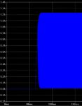
current_source_step_response.JPG

So if I use the stabilising "out of loop" or "in the loop" (can't remember the term) circuit shown here;

https://www.analog.com/media/en/technical-documentation/application-notes/an105fa.pdf

This doesn't work and there is still +75dB @ 180deg phase shift.
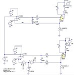
current_source_loop_gain_compensated.JPG

current_source_loop_gain_compensated_margins.JPG

The unknown device is the inductor (10mH) + resistor (200uR), the inductance is causing the problem.

The idea of this circuit is to drive a constant current through a highly inductive low resistance load.

Do you have any advice as to how to compensate this loop?

Thanks!

- - - Updated - - -

P.S - I do not need a fast response, so I would be happy rolling off the gain in the loop early, a 10Hz cutoff would be OK.
 

On the last schematic figure the top feedback amplifier does the same step response?
I couldn't recognize this stability test setup how would operate, I am curious that how the step response looks like without your controlled sources.
..ohh I've just recognized the output MOS can be in triode region if the Vds of it is small and the Ids high...like in your case, that isn't good for stability.
 

Hi frankrose

Thanks for he response, I must say I was a bit concerned about the drive voltage to the gate as the op amp is hitting rail at the start of the plot.

For the transient analysis I was running a separate test with only the top circuit.

During the loop gain analysis I was using the top circuit to obtain a quiescent voltage for the feedback node.

I haven’t worked with Mosfets too much, so I will do some research today about the Triode region, I will post some more transient plots later.

Thanks
 

There are two possible reasons why the current source circuit has instability that doesn't show in your loop gain simulation:
- different output current and thus different MOSFET gm between loop gain simulation and actual operation
- dynamic instability caused by OP and MOSFET large signal behavior

The loop gain "measurement" circuit looks overly complicated to me, I would refer to a simple Middlebrook's setup with a series stimulation voltage source.
 
Hi FvM

Thanks for the response, I also think the loop gain setup for injecting the perturbation is overly compocated but I was having terrible trouble getting sensible measurements with a series injection voltage source. I will try again.

I haven’t actually had a problem with a real circuit yet, but I can’t test (on the bench) all of the possible conditions that the “unknown device” could exhibit.

I think part of the problem is this triode region.

- - - Updated - - -

There are two possible reasons why the current source circuit has instability that doesn't show in your loop gain simulation:
- different output current and thus different MOSFET gm between loop gain simulation and actual operation
- dynamic instability caused by OP and MOSFET large signal behavior

The loop gain "measurement" circuit looks overly complicated to me, I would refer to a simple Middlebrook's setup with a series stimulation voltage source.

But as far as I can tell, the loop gain simulation is showing that the loop is very unstable.
 
Last edited:

Yes, we see that, just we are not sure that the small signal equvivalent explains the large signal oscillation now. We cannot sure this overcomplicated test explains the large signal behaviour.
To move the transistor from triode region to saturation increase the V7 source voltage to 10V for example, should be enough.

Ok got it, I will run some further tests tonight.

I ran a quick simulation today and increasing the voltage source stopped the oscillation.

This causes me a different problem as then the mosfet will have to dissipate huge amounts of power.

I still feel I need to sort out the small signal loop stability as well though, don’t you?

Thanks so much! I really appreciate the advice.
 

But as far as I can tell, the loop gain simulation is showing that the loop is very unstable.
I can't check the loop gain of your circuit because I don't know which transistor model you are using. It's not shipped with Ltspice. See below a simulation with a 100V 8mOhm MOSFET.

MOSFET CS.PNG


The loop gain is cut down by Ciss in combination with low impedance and showing no problems, large signal behavior may be critical, though. I'm posting the schematic primarily to show the loop gain measurement setup.

Before suggesting compensation circuits etc., I would like to understand the application requirements (speed, current range).
 
I checked a similar NMOS in LTSpice, an IRF530 and actually with 1A drain current the Vdsat is low enough, it is under 700mV.
It is strange for me now your circuit cannot operate from 1.25V, you should have enough headroom.
Could be your MOS model the problem here? For example I am not sure about how the MOS operates in this circuit if you swap the drain-source pins on the symbol accientally.
 
I can't check the loop gain of your circuit because I don't know which transistor model you are using. It's not shipped with Ltspice. See below a simulation with a 100V 8mOhm MOSFET.

View attachment 149649


The loop gain is cut down by Ciss in combination with low impedance and showing no problems, large signal behavior may be critical, though. I'm posting the schematic primarily to show the loop gain measurement setup.

Before suggesting compensation circuits etc., I would like to understand the application requirements (speed, current range).

Hi FvM

I have tried to run exactly the same simulation as you but I am having no success, it still shows the loop is unstable.

I used the same components and used your loop gain method, can you take a look to see what I am doing wrong?

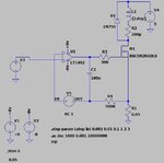
loop_gain_test_circuit.JPG

loop_gain_test_method.JPG

I am still showing huge gain at 180deg phase shift.

- - - Updated - - -

Hi FvM,

I am reading your plot as being unstable, I looked again at my plot and it is the same as yours except I started at much lower frequencies.

At very low frequencies the phase is -180 (perfect negative feedback).

By the time you phase shift by +180deg you are at 0deg (positive feedback) at around 1.29kHz, you still have 60dB don't you?

Or am I misreading the phase plot?

See below where I believe is the zero degree crossover

loop_gain_zero_degree_crossover.JPG

- - - Updated - - -

FvM, if you run a transient analysis on your circuit does it oscillate?

Mine does if i perform a 0.05v pulse with a rise time of 0.0001 and 1 second duration.

- - - Updated - - -

Edaboard won't let me upload my .asc file, is that right?

- - - Updated - - -

Edaboard won't let me upload my .asc file, is that right?
 

I apologize for not looking closely at the phase response. You are absolutely right, the circuit in post #8 has negative phase margin. Compensation network like below required.

MOSFET CS2.PNG

The problem behind the low stable loop bandwidth is the large OP output impedance, respectively lack of capacitive load driving capability.
 

Wow!

FvM please do not apologise, this is a brilliant learning exercise for me.

Thank you, but do you have any reference for me to look at so that I will be able to perform this type of compensation myself with different output impedances and mosfets?

Thanks!

- - - Updated - - -

To give you some background;

I will have number differnet shunts;

0.003
0.05
0.5
5
50
500

The load will be of an unknown inductance (could be up to 5H max, unlikely but I want to achieve stability up to this theoretical value), but the resistance of the load will be constrained within the following limits (connected between the drain and the main voltage source)

0~20u Ohm (0.003 Ohm shunt)
20u~200u Ohm (0.05 Ohm shunt)
200u~2m Ohm (0.5 Ohm Shunt)
2m~200m Ohm (5 Ohm shunt)
200m~2 Ohm (50 Ohm shunt)
2~200 Ohm (500 Ohm shunt)

Each shunt will have its own mosfet driver and its own op amp, so they can be individually compensated for the respective loads.

I would like to know how you calculated the compensation values so that I can apply your method to the other shunts.
 

do you have any reference for me to look at so that I will be able to perform this type of compensation myself with different output impedances and mosfets?
Unfortunately not, may be others have suggestions.

I concede that the rather low compensation network corner frequency of about 3 kHz is counter-intuitive at first sight for a 3 MHz OP. But it's actually required to bypass and "neutralize" the weird transfer function of the MOSFET with output load. There are other possible ways to "tranquilize" the circuit, e.g. a RC snubber in parallel to the output inductance.

If your application requires a higher current source bandwidth, an OP with higher bandwidth and lower output impedance would be required.

Ok no problem, but how did you come up with those values, did you perform hand analysis?

Or was it a “stab” :)
 

Just from curiousity, but how is the step-response with 1.25V drain voltage? Was it solved? If not, and the compensation method is finalized I would mention that you can connect paralel MOS devices to decrease the Vdsat. It will increase the output headroom, the gate capacitance, but with the correct compensation last shouldn't be a problem.
 

Just from curiousity, but how is the step-response with 1.25V drain voltage? Was it solved? If not, and the compensation method is finalized I would mention that you can connect paralel MOS devices to decrease the Vdsat. It will increase the output headroom, the gate capacitance, but with the correct compensation last shouldn't be a problem.

Hi frankrose

It’s a good question, I am going to test that today.

I still think it’s in the triode region when the current is first turned on because of the large initial voltage drop across the inductance.

Once the current builds and the di/dt falls off to a steady state DC, the overall voltage drop across the load falls away (to only be the voltage drop across the small resistance) and it will no longer be in the triode region.

I will post some transient response results today of the gate voltage, DUT voltage and the current.

I think I have found a reference to use which seems to apply the same “in the loop” compensation that FvM has applied.

I will try to use the technique described in this article; https://www.analog.com/en/analog-dialogue/articles/techniques-to-avoid-instability-capacitive-loading.html

I will see how I get on.

- - - Updated - - -

Oh and one point I forgot to mention is that I only need a bandwidth of 3kHz.

I will look for a better op amp too.
 

The limiting factors for stable current source bandwidth are OP output impedance, OP bandwidth and MOSFET Ciss.

I didn't yet hear a specification of maximal output current, you should select a suitable MOSFET with sufficient but not overly low Rdson. Also with Vds,max according to the maximal required output voltage. A 100 V MOSFET isn't a good choice.

That’s a good point, I don’t need a 100V mosfet.

Max current using the 0.003 Ohm shunt is 10A.

I will look for a Mosfet with a lower threshold voltage and hopefully lower Ciss, I just need it to be able to dissipate 15W continuously. I have plenty of room for a huge heat sink, but it is still a concern.

I think I can apply the compensation techniques in my previous post (Analog devices article), but will also look for an op amp with lower output impedance.
 

Hi all

I thought I would make another post, I wanted ot get your opinion on the loop responses from these two circuits.

Looking at FvM's circuit, I am a little worried about the phase "dipping" early in the plot to around 2deg.

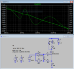
graph_2nF.JPG

If I change the values to the following;

100nF_Cf.JPG

I get this response, with minimum phase of 39deg.

I know phase margin is taken at 0dB, but shouldn't I be worried about what the phase is doing (if it gets close to 0deg) earlier in the sweep?

Also, I think I will try this MosFet, it has much lower threshold and will be fine as far as my power requirements are concerned.

https://www.infineon.com/dgdl/irf1324pbf.pdf?fileId=5546d462533600a4015355dac93318a7

Any objections to my higher value of C1 and R3?

I am using "empirical" methods to choose the values of the compensation network, is that "OK" providing I get a stable circuit? I can't see the point of applying lots of maths if the circuit is stable.

Thanks!

graph_Cf_100nF.JPG

I get
 

You don't have to worry about the 39° phase margin before zero crossing, your circuit will be stable. To get exact mathematical answer the simulation is the best combined with empircial considerations. This is the engineering way. If you don't write a thesis and don't want to spend time with basic small signal modeling there is no rule you must. Not a disadvantage if you do, but not necessary.
 

Status
Not open for further replies.

Part and Inventory Search

Welcome to EDABoard.com

Sponsor

Back
Top