Continue to Site

Welcome to EDAboard.com

Welcome to our site! EDAboard.com is an international Electronics Discussion Forum focused on EDA software, circuits, schematics, books, theory, papers, asic, pld, 8051, DSP, Network, RF, Analog Design, PCB, Service Manuals... and a whole lot more! To participate you need to register. Registration is free. Click here to register now.

If anybody need help in EAGLE, ask me in this POST !

Status
Not open for further replies.
Hi

I need to do track reinforcement with solder to alow more current in track and I don’t know how to open the solder stop mask to do that.

I am using version 5.60 of Eagle by now and I am a basic user, so please, take it in account in your explanation.

Thank you very much in advance
 

Simply draw a track over the copper in the solder mask layer. The solder mask layer is a negative layer - where you draw you WON'T get solder mask.

Keith
 

Thank you for your answer.
Sorry about my duplicated post – my mistake.:oops:

Well, I am using a polygon for high current large track, but I am sure it is not enough. So, I need do reinforcement with solder in this polygon in the solder machine. I just tried you suggestion and when I check the gerber STS file in ViewMate the solder mask still there.

Tks in advance
Ronaldo
 

Are you sure the solder mask is there? It is a negative so where you see soldermask layer in the Gerbers it is actually missing. Post the Eagle files and I can check you have done it correctly. It does work!

Keith.
 

I did what you told in N$5 net from attached BRD file.
I also attached a picture of what I hope to get.

Regards and thank you
Ronaldo
 

Attachments

  • Triac_Line_In.rar
    9.2 KB · Views: 105
  • imgCAIFEM0W.jpg
    imgCAIFEM0W.jpg
    23.8 KB · Views: 119
Last edited:

I cannot see it! I have drawn what I think you want on layer 30. Turn off all layers except 30 to see it clearly - I drew it as a layer 30 track over the layer 16 track.

As a separate issue - your tracks don't actually connect to the pins. Also, if you are planning to put a wire over the track you might want to make the ground plane further away from the tracks (increase the clearance) to minimise the risk of shorts.

Keith.
 

Attachments

  • Triac_Line_In-mod.zip
    10.1 KB · Views: 112
Thank you very much about my question and your tip.
Regards from Brazil
Ronaldo
 

One other tip - copy the tracks then change the layer to layer 30. Then they will be in exactly the right place.

Keith
 

Here it is. I haven't made the pads "pointy" like the Coilcraft footprint, but I don't believe it is critical - I have used the footprint a few times.

Keith.
 

Attachments

  • LPD4012.zip
    1.1 KB · Views: 109
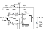
sorry to ask some stupid qns... for package TO220 horizontal there are 3 pins but in the schematic(Attachment LM1085.png) there are 4 connections coming out of the component LM1085. Does it mean that i have to connect a wire to the tap?

I am trying to create the library for SMA862P-0000. I have the datasheet attached and library file i made but im not sure if it is correct. Could someone help me see if it is correct? And what kind of symbol should i use for this kind of connector. Is it usually the case that the 2 connections( the bigger pads...top and bottom) are usually grounded?
 

Attachments

  • LM1085.png
    LM1085.png
    11.4 KB · Views: 106
  • testlibrary.zip
    995 bytes · Views: 111
  • SMA862P-0000.pdf
    190.9 KB · Views: 131

You don't have to actually connect to the 4th terminal - it is the same as the output - middle leg. If you stand up the TO220 and use a heatsink clipped or bolted to it then you wouldn't use the fourth connection. If you laid it on the PCB then you may choose to use it. Look at the various TO220 variants in the "ref-packages" library.

While there are a few SMA connectors in the standard libraries (look in "con-coax"), I cannot find one exactly like yours but that is probably because that connector is panel mount not PCB mount. I suggest you use a PCB mount connector or connect the one you have suggested through some coax cable.

Keith.
 
  • Like
Reactions: wongwk

    wongwk

    Points: 2
    Helpful Answer Positive Rating
hi, I want to make a QFN package (TPS61200) to a generic DIP10 packaging footprint in a PCB, the problem is, in Eagle, i'm having a hard time try to connect all the pads of the QFN to DIP since the pads are close to one another, anybody can help me with this?
 

I am not quite sure what you are trying to do. Are you trying to make a footprint that will take a DIP and QFN package? (the TPS61200 is not available in DIP, so I am not sure why you would want to do that). If so, it should be possible. The QFN is 3mm wide. The pitch of a DIP package is 7.6mm. Even with the pads required on a DIP that still leaves plenty of room to place the tracks. Maybe you could post and image of what your problem is, or the Eagle file.

Keith.

I'm trying to make a QFN to DIP adapter specifically for the TPS61200 so that I can test it out on a breadboard with jumpers for connections, etc.. my problem is connecting the pads of the QFN to all the pins of the DIP package because what I'm thinking of is the QFN being in the middle of the DIP rows..
 

I put a QFN in between the legs of a DIP and it looked fine. Make sure your DIP pads are round and not oversized. Use small tracks.

Keith
 

I need to design a PCB with a NE34018 transistor, but I can't find any model which uses the same package (SOT-343). Where can I find it?
 

Status
Not open for further replies.

Part and Inventory Search

Welcome to EDABoard.com

Sponsor

Back
Top