Continue to Site

Welcome to EDAboard.com

Welcome to our site! EDAboard.com is an international Electronics Discussion Forum focused on EDA software, circuits, schematics, books, theory, papers, asic, pld, 8051, DSP, Network, RF, Analog Design, PCB, Service Manuals... and a whole lot more! To participate you need to register. Registration is free. Click here to register now.

If anybody need help in EAGLE, ask me in this POST !

Status
Not open for further replies.
Could you post the schematic? It isn't because you added junctions later, but can be if you have doubled back on wires.

Keith.
 

Schematics sent to your inbox, thanks.
 

Thanks. I have had a look and it is simply where two lines cross but are not connected. If you double click on the errors it will show you where they are. This is a "feature" in more recent versions. I guess they have tried to improve the ERC coverage, but all it does is create more warnings. However, if you "approve" them after checking then they shouldn't appear next time you check.

Keith.
 

Approved :)

Thank you.
 

Hi

how can i export the PCI-E-164 connector from con-pc library to pads layout ?!

thanks in advance
 

Do you mean for the Pads layout software? If so, I am not sure that you can. You can export data from libraries to import into other Eagle libraries.

Keith.
 

Hi, can anyone give advice on how to create a land pattern for a circulator in Eagle?

I can't find any packages that look like a circulator in existing libs, and the datasheet does not specify the land pattern very well. Mainly they don't say anything about layers, soldermask or pad size. I could calculate the size of the pins from the package layout, but how can I decide the size on pads in the land pattern?

I'm a rookie at making land patterns, but I have made a few from datasheets where dimensions and layers are well specified. So if anyone could give their viewpoint and advice on how to make this I would be very greatfull!

Have a look at the datasheet, just google "Dorado 3CDMG35-4". (dont know how to upload :p)

Regards,
Alex
 

That is a weird thing to surface mount. It is not clear from the datasheet whether you need to connect the large ground area or not. For the three other pads I would make something which is slightly larger than the circulator pad "sideways" and towards the centre, and quite a bit longer radially, if that makes sense. The reason for that is so if you want to hand solder it you have something to get your soldering iron on to.

It may be worthwhile contacting the manufacturer to see if they have a recommended land pattern.

Keith.

Added after 6 minutes:

Actually, just noticed that the last part of the data sheet is the recommended land pattern! It is a bit short of dimensions, but seems to suggest the ground should be exposed copper with 23 0.8mm vias. Their recommended land width is very narrow - only as wide as the notch in the connection.

When I have created similar things, I have just put the ground pad on the footprint and added the vias in the layout. That does give you a load of errors in the DRC though. I am not sure if there is a better way. You could add loads of vias connected to ground onthe actual footprint, but you also need a large pad as well. I think you may still get errors in the DRC, although there may be a better way with the alter version of Eagle - I am still running 4.16r2

Keith.
 

Thank for a quick answer Keith, really appreciate it.

To be honest, this is the first time I'm making a board, Im just a student and we've not done this before in classes. I'm making a "prototype" front end of a radiometer for my masters degree.

I really don't know what's wierd and what's not in this world, but the circulator IS an smd device, so how else to mount it? =P

Anyways,
I've reasoned, as you said, that the main land of the device should be exposed copper, and the solution about using vias in the PCB design was also an idea I had, as I've done that with some QFN packages.

The problem is as you've noticed, the lack of dimensions. How am I supposed to figure the size of the pads?

More questions: Should I apply soldermask anywhere? Should I use solder paste in the middle, and should I add that in tCream as a circle with corresponding diameter to the device land pattern? Or do I only need a copper layer, and add the vias?

I am more or less left to my self to work out some of these problems in the design, because, frankly, there are no one else working on this stuff at the faculty atm.. :S

Seems I might just have to gamble on the pads ... or wait until I actually get that damned thing, which might take a while, and take physical measures.

I'm using Eagle 5.8.0 light, but as I said, I'm a rookie with little experience.. this is a massive task for me ;P
 

With new components if you are unsure - buy one first. That is what I often do. You can then print your layout and plonk the part on and make sure you have it right. If that will create too much of a delay then you will have to guess. I don't think it is a big risk really - just measure the drawing in the data sheet to get a rough idea where the pads are and what would be a suitable width. You may want to make the pad width the correct one for 50ohms, depending on how that works out.

My concern about it being "surface mount" is how you get the solder paste underneath it to melt. Maybe your PCB assembler could comment.

If you use a circular pad for the underside then it will automatically add the paste & solder mask layers correctly. If you make it out of copper you will need to add them. I would just use an SMD pad of the right size and use 100% roundness - then it will be round (roundness rounds off the corners).

I use Eagle a lot and like you I have used QFN pads with pads underneath and some "power" SO/TSOP ones have them, but I have never made anything with such a large pad.

Keith.
 

Thanks again Keith.

I've had some contact with the Dorado sales office in Sweden, but I haven't got an answer on the lead time .. So it may take a while to get the device :/

Anyways, to get going on the design I just designed a "prototype" device to use, as I need to get going on how to design the PCB layout. I used the SMD pad and rounded it off as you said, and then I added pads that have the same width as the traces. I use a Rogers RO4350b laminate, and the traces are about 0.52 mm. I'm unsure about the length of the pads, but the mounting pins seem to be quite large and stick out some from the device, so I made them 1.55 mm long.

At least I can get started on the design :)
 

As long as you get the pads radially in the correct place it doesn't really matter. It makes more of a difference when you want a production device to be re-flow soldered. Personally I would probably make the pads a little longer to give you a bit more to solder to, and minimise the risk of them being totally hidden under the pads. Maybe 3mm.

Keith.
 

I have placed rectangles in layer 17 for pads that I ONLY need on the top layer. I have more pads that I need on the bottom layer. If I place them all in layer 17, then my gerber files will be messed up when I select them. Do you have any advice on how to get pads on top OR bottom layers?
 

Do you mean surface mount pads? Are you creating a library or a PCB? Layer 17 is only for the pads of through hole components. Surface mount components have SMD pads places all on the top layer (1) in the library editor. Then when you mirror them when designing the PCB they appear on the bootom layer (16).

Keith.
 

yes, Surface mount pads. I am creating a PCB. My problem is that I need to place individual pads on both the top and bottom layers. the 2 need to remain seperate however
 

You should really use footprints, not individual pads. If you do use pads they should be SMD ones on layers 1 and 16, not layer 17 which is for through hole.

Keith
 

I am new to EAGLE/ PCB designing in general. What is a footprint and how do i use them?
 

Maybe have a look at this, and some of the other pages related to Eagle on that site:

https://www.instructables.com/id/Draw-Electronic-Schematics-with-CadSoft-EAGLE/

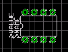
In all PCB software you would normally work with parts both in the schematic and the layout. So, if a component has 8 pins you work with a schematic symbol with 8 pins and on the layout with a "footprint" with 8 pins. You don't normally place the pins individually. So, for an 8 pin DIL part you would work with a footprint like this:

54_1280753683.gif


It will also contain an outline of the part and the component reference (name) and optionally other information such as the value.

Keith.
 

You still around Keith? =)

I had to take a break on the PCB design. I'm still unsure about the darn circulator from a few posts back...

I'll try to break down the case in point:

* i have some QFN packages. In those, to ground the pads that should be grounded properly, I leave the pins without thermal and connect to ground.

* The ground pad of the device is just specified by a square of cream and stop layer. Via to ground are added in the PCB drawing.

* Now, I have a ground plane on the top and bottom. Specified by making two polygons around the board, one top, one bottom, then naming them GND.

* I then use rastnest, and this is what happens:

* For the pins on various packages that are connected to ground, they are simply left open.. red on red (gnd on gnd)

* Pins that belong to the signal are shielded off, visualized by a blue outline.

* Ground planes (mid paddle) of QNF package such as the LNA being just cream are now in direct contact with the top GND layer. I further add vias to bottom ground.

This is how the last board using similar devices was made. And it works.

The last PCB did not use circulators however. And now I see a potential problem, but I am unsure.

* As I use a SMD to make the circular ground plane, even if I leave off thermal, eagle thinks the center pad belong to the signal, not GND. Thus, the entire circle is outlined by a shielding blue area, as if it were a signal path.

Will it work to just add tons of vias?

I have gotten a better proposal of land pattern from the manufacture. On it it says the following:

"To ensure proper electrical and thermal performance there must be a ground plane of 100% solder connection underneath the part".

The drawing also shows how to place vias (thru holes to gnd) on the center pad.

If this did not make sense please do ask me to clarify :)
 

I think the easiest thing to do would be to send me the Eagle schematic & PCB file - I got lost halfway through your post! A picture will (hopefully) tell a thousand words.

Keith.
 

Status
Not open for further replies.

Part and Inventory Search

Welcome to EDABoard.com

Sponsor

Back
Top