Continue to Site

Welcome to EDAboard.com

Welcome to our site! EDAboard.com is an international Electronics Discussion Forum focused on EDA software, circuits, schematics, books, theory, papers, asic, pld, 8051, DSP, Network, RF, Analog Design, PCB, Service Manuals... and a whole lot more! To participate you need to register. Registration is free. Click here to register now.

I2C operation how master recognise a slave

Status
Not open for further replies.
PA3040 said:
Please explain what is the meaning of general call condition in I2C

The general call address is used to do broad cast over the entire bus. It addresses all the slaves connected to the bus irrespective of their programmed address. But it is not mandatory that all the connected devices should respond to general call addressing. The devices that not interested in general call can ignore the same. But those devices make use of general call should acknowledge properly. The byte follows the general call address usually define what action needs to be taken by the slaves in response to the call. The command in the second byte is interpreted based on the value of its LSB. If LSB is zero, the following commands are defined.

00000110 (0x06): When receiving this command, all devices should reset and take in the programmable part of their address.
00000100 (0x04): Take in the programmable part of the address, but do not reset

Other values in this scenario are undefined and should be ignored by slaves.

When the LSB of the second byte in general call is one , it means that this call is made by a hardware master device who does not have any prior information of the connected slave addresses. In this case the master does the call with its own address so that the slaves can identify the source of the message.

I2C Bus: General Call Address
**broken link removed**
An I2C Tutorial.
**broken link removed**
 
  • Like
Reactions: PA3040

    PA3040

    Points: 2
    Helpful Answer Positive Rating
i2c.JPG

Dear All
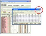
Above picture shows simulator how read & write to EEPROM using I2C.here slave address is 4 bits but manual says it is 7bits. then how can we load slave address to SSPBUF register

as well as please advice to me can we simulate I2C using MPLAB SIM
 

Above picture shows simulator how read & write to EEPROM using I2C.here slave address is 4 bits but manual says it is 7bits. then how can we load slave address to SSPBUF register

The address counter you have circled in the attached picture is the internal memory address of the serial EEPROM, not the address of the serial EEPROM device itself. The address range of an I2C serial EEPROM is dependent solely on the storage capacity of the serial EEPROM, ranges of a few kilobits to one megabit are typical, notice these values are in bits therefore for a byte oriented device you must divide them by eight to arrive at the storage capacity of the device in bytes.


as well as please advice to me can we simulate I2C using MPLAB SIM

The MPLAB SIM modeling language SCL is very similar VHDL, to simulate an I2C device would require writing a SCL routine, a nontrivial task. You maybe able to use a stimulus data file to mimic the contents of an I2C Serial EEPROM combined with a I2C SCL routine.

SCL PRIMER / TUTORIAL

SCL Code repository

Coding directly in SCL\SCL as VHDL subset

Hope the info helps in your endeavors,

BigDog
 
  • Like
Reactions: PA3040

    PA3040

    Points: 2
    Helpful Answer Positive Rating
Dear BigDog

as per my picture. let me know the address that i want use here

this is 24c32 eeprom 1010 A1 A2 A3
 

as per my picture. let me know the address that i want use here
this is 24c32 eeprom 1010 A1 A2 A3[

The picture above fails to give any indication of how the 24C32 EEPROM's address is set. As you've indicated in your posting above, the devices address is comprised of 1010A2A1A0 the state of the external address lines A2, A1 and A0 must be determined before the device's actual address is defined. For example if all three external address lines were tied to ground (GND) the devices address would be 1010000.

Reference 24C32 32K 5.0V I2C™ Smart Serial™ EEPROM Datasheet, pg 5, Section 3.6 Device Addressing

A control byte is the first byte received following the
start condition from the master device. The control byte
consists of a four bit control code; for the 24C32 this is
set as 1010 binary for read and write operations. The
next three bits of the control byte are the device select
bits (A2, A1, A0). They are used by the master device
to select which of the eight devices are to be accessed.

Once the device's address is determined the control byte can be formed and used in conjunction with device commands for read/write operations.

How is your particular device's external address lines configured?

BigDog
 

Dear BigDog Thanks for reply
How is your particular device's external address lines configured?

it does not show how configure external pins, it show configure SCL and SDA line only

can you see any error the program I wrote for I2C

Code:
status		equ		0x03	;bank 0
intcon		equ		0x8b	;bank 0
pir1		equ		0x0c	;bank 0
sspbuf		equ		0x13	;bank 0
sspadd		equ		0x93	;bank 1
sspcon		equ		0x14	;bank 0
sspstat		equ		0x94	;bank 1
trisc		equ		0x87	;bank 1
portc		equ		0x07	;bank 0
sspcon2		equ		0x91	;bank 1
i2c_addres	equ		b'10100000'		;24c32 address


start		call	sys_init
			clrwdt
			goto	main
main		call	i2c

i2c			bcf		intcon,7
			call	i2c_start
			movlw	i2c_addres
			addlw	b'11111110'
			call	tx_byte
			call	is_ackn_rx
			movlw	0x00
			call	tx_byte
			call	is_ackn_rx
			call	i2c_restart
			movlw	i2c_addres
			iorlw	b'00000001'
			call	tx_byte
			call	is_ackn_rx


i2c_start	bsf		status,5
			bsf		sspcon2,0
			bcf		status,5
			bcf		pir1,3
			btfss	pir1,3
			goto	$-1
			bcf		pir1,3
			return
		
i2c_restart	bsf		status,5
			bsf		sspcon2,1
			bcf		status,5
			bcf		pir1,3
			btfss	pir1,3
			goto	$-1
			bcf		pir1,3
			return

tx_byte		clrwdt
			bcf		pir1,3
			movwf	sspbuf
is_tx		        btfss	        pir1,3
			goto	is_tx
			bcf		pir1,3
			return
			
is_ackn_rx	bsf		status,5
ack_rx_loop	clrwdt
			btfsc	sspcon2,6
			goto	ack_rx_loop
			bcf		status,5
			return
			
sys_init	bsf	status,5
			movlw	b'11111011'
			movwf	trisc
			bcf		sspstat,7
		;	bsf		sspstat,3
			bcf		status,5
			movlw	b'00101000'
			movwf	sspcon
			
			return
end
 
Last edited:

Dear BigDog Thanks for reply


it does not show how configure external pins, it show configure SCL and SDA line only

can you see any error the program I wrote for I2C

Code:
status		equ		0x03	;bank 0
intcon		equ		0x8b	;bank 0
pir1		equ		0x0c	;bank 0
sspbuf		equ		0x13	;bank 0
sspadd		equ		0x93	;bank 1
sspcon		equ		0x14	;bank 0
sspstat		equ		0x94	;bank 1
trisc		equ		0x87	;bank 1
portc		equ		0x07	;bank 0
sspcon2		equ		0x91	;bank 1
[COLOR="#FF0000"]i2c_addres	equ		b'10100000'		;24c32 address[/COLOR]


start		call	sys_init
			clrwdt
			goto	main
main		call	i2c

i2c			bcf		intcon,7
			call	i2c_start
			movlw	i2c_addres
			addlw	b'11111110'
			call	tx_byte
			call	is_ackn_rx
			movlw	0x00
			call	tx_byte
			call	is_ackn_rx
			call	i2c_restart
			movlw	i2c_addres
			iorlw	b'00000001'
			call	tx_byte
			call	is_ackn_rx


i2c_start	bsf		status,5
			bsf		sspcon2,0
			bcf		status,5
			bcf		pir1,3
			btfss	pir1,3
			goto	$-1
			bcf		pir1,3
			return
		
i2c_restart	bsf		status,5
			bsf		sspcon2,1
			bcf		status,5
			bcf		pir1,3
			btfss	pir1,3
			goto	$-1
			bcf		pir1,3
			return

tx_byte		clrwdt
			bcf		pir1,3
			movwf	sspbuf
is_tx		btfss	pir1,3
			goto	is_tx
			bcf		pir1,3
			return
			
is_ackn_rx	bsf		status,5
ack_rx_loop	clrwdt
			btfsc	sspcon2,6
			goto	ack_rx_loop
			bcf		status,5
			return
			
sys_init	bsf	status,5
			movlw	b'11111011'
			movwf	trisc
			bcf		sspstat,7
		;	bsf		sspstat,3
			bcf		status,5
			movlw	b'00101000'
			movwf	sspcon
			
			return
end

How did you arrive at the I2C device address of "10100000"? Assuming all external pins are tied to GND, the address should be "01010000" due to the fact the actual device address is only 7-bits long.

BigDog
 
  • Like
Reactions: PA3040

    PA3040

    Points: 2
    Helpful Answer Positive Rating
Dear BigDog
Thanks I got it
I edited it but problem remaining same. the simulator does not response any
My simulator is PIC SIMULATOR IDE v6.65
 

in software you have to send address like A0 for 1st eeprom A1 for second like that..
like this depending on the software you send to slave that particular slave will talk to master controller...
hope you understand.


As per above, that mean we not need any hardware configuration for A0 , A1 , A2 ( this mean this pin renaming open , am I right)?
 

As per above, that mean we not need any hardware configuration for A0 , A1 , A2 ( this mean this pin renaming open , am I right)?

No, they need to be tied to either GND or Vdd, with the desired address of 01010000 to GND.

Address lines as a general rule should not be left floating.

I'll examine your code indepth later today.

BigDog
 
  • Like
Reactions: PA3040

    PA3040

    Points: 2
    Helpful Answer Positive Rating
You should tie A0, A1 and A2 to Ground or Vcc. You can have a total of 8 combinations. They are given below:

Code:
A2          A1          A0

0            0            0                   (Here device address becomes  1010000 (7 bit address) 

0            0            1                   (Here device address becomes  1010001 (7 bit address) 

0            1            0                   (Here device address becomes  1010010 (7 bit address) 

0            1            1                   (Here device address becomes  1010011 (7 bit address)

1            0            0                   (Here device address becomes  1010100 (7 bit address)

1            0            1                   (Here device address becomes  1010101 (7 bit address)

1            1            0                   (Here device address becomes  1010110 (7 bit address)

1            1            1                   (Here device address becomes  1010111 (7 bit address)


0 means Connected to Ground
1 means Connected to +Vdd
 
Last edited:
  • Like
Reactions: PA3040

    PA3040

    Points: 2
    Helpful Answer Positive Rating
i2c11.JPG

Dear all

see picture
Cam anybody explain what is the meaning of I2C Firmware controlled Master mode (slave idle)
 

The I2C Firmware controlled Master mode (slave idle), is the most common I2C mode used by a MCU. The MCU is designated as Master of the I2C bus and is responsible for generating clocking and issuing commands. The master of an I2C must generate the clock signal, the slave cannot which is why it is referred to as "idle". The transmission and clock signal are started when data is written to SSPBUF, the BF bit is set as well and cleared once the byte has been transmitted.

There are some I2C which can act as Master of an I2C bus, however most peripheral I2C devices act as slaves. One common exception is connecting two or more PICs or other MCUs together via the I2C bus as a communications channel one MCU is usually delegated as Master and the rest of the MCUs slaves.

Does this info help,

BigDog
 

Dear bigdog
really and really thanks for your reply
I sow this reply in Google. now I am bit confuse

I have some ideas, what this mode could be, but I am not shure:
Lets assume, that in this mode the I2C module is disabled (SSPSR does
not shift, WCOL, SSPOV, BF (and the other flags) are not touched .. and
so on...). The only part of the I2C module, that is enabled is the START
and the STOP detector. Both trigger an interrupt. All I2C bus operations
are done through software, manipulating PORTC. --- But if one realizes a
I2C master doing so, START/STOP interrupts are not nessecary, because
the I2C master drives START/STOP. It could be helpful, if one whishes to
realize a I2C slave in software, but this way this mode would not be
called a "master mode".
So I am a little bit confused about the basic function of this mode
 

The person quoted above is discussing the implementation of an I2C interface as a Master device using software methods rather than a I2C hardware module. This software only method is often referred to as a softI2C or bit-banged I2C, this technique is often deployed with devices which lack the required hardware peripherals or modules required for an specific task.

By the way, what model PIC you are using in your design?

BigDog
 
Dear BigDog,
Thank you so much for reply

I am still confusing and my MCU is 16f877a
can i have any link that explaining this matter
Thanks
 

The I2C Firmware controlled Master mode (slave idle), is the most common I2C mode used by a MCU. The MCU is designated as Master of the I2C bus and is responsible for generating clocking and issuing commands. The master of an I2C must generate the clock signal, the slave cannot which is why it is referred to as "idle". The transmission and clock signal are started when data is written to SSPBUF, the BF bit is set as well and cleared once the byte has been transmitted.

There are some I2C which can act as Master of an I2C bus, however most peripheral I2C devices act as slaves. One common exception is connecting two or more PICs or other MCUs together via the I2C bus as a communications channel one MCU is usually delegated as Master and the rest of the MCUs slaves.

Dear Big
That mean The I2C Firmware controlled Master mode (slave idle) is. if slave has capability to act as a master but in this configuration, that capability
will disable in the slave
 

Hi all,

how the clock is generated for firmware controlled master mode?

1011 = I2C Firmware Controlled Master mode (slave Idle)
1000 = I2C Master mode: clock = FOSC/(4 * (SSPxADD + 1))


for 1000 mode clock equation is given in datasheet but for 1011 mode how can we select the I2C clock
 

Status
Not open for further replies.

Similar threads

Part and Inventory Search

Welcome to EDABoard.com

Sponsor

Back
Top