Continue to Site

Welcome to EDAboard.com

Welcome to our site! EDAboard.com is an international Electronics Discussion Forum focused on EDA software, circuits, schematics, books, theory, papers, asic, pld, 8051, DSP, Network, RF, Analog Design, PCB, Service Manuals... and a whole lot more! To participate you need to register. Registration is free. Click here to register now.

[SOLVED] How to include a modification in a PIC dev board with PIC16F877A for OVP ?

Status
Not open for further replies.
suggestion:
add three pull-up resistors (10K) from A0, A1 and A2 on the PCF8575 and also add three 'jumper' links to ground from them. That will ensure the address is fixed and allow it to be changed if more I2C devices are connected to RC3 and RC4. It makes it more versatile.

I would advise you to change 'VCC' to a more suitable name, maybe "Vin" to avoid confusion with the VCC pins on some ICs where it is the 5V supply. On your schematic VCC is whatever comes from the external power supply.

Add a resistor (suggest 47K) between RB0 and 5V. This is because the PCF8575 INT pin can only pull the line low. If RB0 is left floating you will get random levels on it and false interrupts will occur.

Change R1 and R2 to 4.7K as per manufacturers recommendations.

Add a 100nF capacitor between the 'In' pins of both regulators to their GND pins as close to the regulators as you can manage.
Add 100nF capacitors across the VCC/VDD pins of the other ICs and their GND/VSS pns as well, again as close to the IC as you can manage.

Other ideas:
The LCD backlight draws several mA which you connected to 5V, this means it comes through U2. As the backlight doesn't need a regulated voltage, you can add a series resistor and connect it to the incoming power instead. It only adds one resistor but saves quite a lot of current.

At the moment any current you draw through the 3.3V regulator also has to pass through the 5V regulator. If you feed it's input from the point you call VCC instead, through a diode it will increase the load you can place on it.

Brian.
 
suggestion:
add three pull-up resistors (10K) from A0, A1 and A2 on the PCF8575 and also add three 'jumper' links to ground from them. That will ensure the address is fixed and allow it to be changed if more I2C devices are connected to RC3 and RC4. It makes it more versatile.

I did that and I used those DIP switches, but I don't think I would use multiple I2C modules because, actually this design has cleared some stuff to me, it's too much for the course.


Add a resistor (suggest 47K) between RB0 and 5V. This is because the PCF8575 INT pin can only pull the line low. If RB0 is left floating you will get random levels on it and false interrupts will occur.

but won't this be a problem that RB0 would be pulled up all the time ?
for this reason I have thought of an idea, that is to put a switch with a red LED on each unit on the dev board to enable/disable it from getting unwanted signals that is going to another unit that is sharing the same IO lines ? and that is by putting the switch with the VCC line.

Another interesting idea I got from a design on github, which is to use a 74HC573 LATCH IC to distribute the directed signal to the targeted onboard unit.
On this link:
BK300-Pic16f877A-development-Board

Change R1 and R2 to 4.7K as per manufacturers recommendations.

Which ones ? the ones with the pullup switches or which ?

Add a 100nF capacitor between the 'In' pins of both regulators to their GND pins as close to the regulators as you can manage.
Add 100nF capacitors across the VCC/VDD pins of the other ICs and their GND/VSS pns as well, again as close to the IC as you can manage.

Yep I did them and also edited the power section.

Other ideas:
The LCD backlight draws several mA which you connected to 5V, this means it comes through U2. As the backlight doesn't need a regulated voltage, you can add a series resistor and connect it to the incoming power instead. It only adds one resistor but saves quite a lot of current.

At the moment any current you draw through the 3.3V regulator also has to pass through the 5V regulator. If you feed it's input from the point you call VCC instead, through a diode it will increase the load you can place on it.

Brian.
I edited the lines and disconnected the feed from 5V regulator. Now both regulators are fed from Vin.

Connected USB line to 5V regulator output line, but there's a problem with this arrangement

But should the USB input voltage need some capacitors ?


Schematic_pic16f877a_dev_board_2020-12-13_12-40-23.png
 
Last edited:

Almost right!
1. A0, A1 and A2 on the PCF8575 don't need R12, R13 and R14 but they should be wired to pins 4, 5 and 6 on the address switch. The R9, R10 and R11 will make the pins high unless the switch is closed to ground one or more of them. It is worthwhile doing to avoid address clashes if other I2C devices are connected to RC3 and RC4.

2. You have wired a resistor in series with VEE on the LCD module, the way it is wired will give you zero contrast setting so nothing will be visible. instead, connect VEE to the wiper of a potentiometer with one end grounded and the other at 5V, the control will let you set the contrast to a suitable level. If you intended to limit the current to the backlight as I suggested earlier, the resistor goes in series with the 'A' pin (Anode of the backlight LEDs).

3. You have added U5, but not connected VDD to it and the capacitor between GND and A2 should be between GND and VDD.

R1 and R2 are the pull up resistors on the SDA and SCL lines, they are needed for the I2C bus to work.

You can connect V_USB directly to 5V, they should both have 5 volts on them but be careful because if you provide external power (through PWR_IN1) the regulated 5V will also appear on the USB socket and therefore could feed backwards to anything plugged in to the USB socket. You could avoid this by using a three pin header and jumper so only one or the other can be used at a time. Like A - B or B-C but avoiding A -C.

Brian.
 
Almost right!
1. A0, A1 and A2 on the PCF8575 don't need R12, R13 and R14 but they should be wired to pins 4, 5 and 6 on the address switch. The R9, R10 and R11 will make the pins high unless the switch is closed to ground one or more of them. It is worthwhile doing to avoid address clashes if other I2C devices are connected to RC3 and RC4.

yes, actually from my experience working with I2C modules for Arduino sketches and some projects I did, the I2C address for that module is fixed and also known in web blogs, tutorials .. etc. for module. But you're right it's better to include those pullups and dip switches.

2. You have wired a resistor in series with VEE on the LCD module, the way it is wired will give you zero contrast setting so nothing will be visible. instead, connect VEE to the wiper of a potentiometer with one end grounded and the other at 5V, the control will let you set the contrast to a suitable level. If you intended to limit the current to the backlight as I suggested earlier, the resistor goes in series with the 'A' pin (Anode of the backlight LEDs).

ok, I chose the resistor to be 330ohm arbitrary and also put a series one with the pot of the contrast pin, how would you think is it a necessary one ?

3. You have added U5, but not connected VDD to it and the capacitor between GND and A2 should be between GND and VDD.
oh ! what a mistake !
I got that thanks ..

R1 and R2 are the pull up resistors on the SDA and SCL lines, they are needed for the I2C bus to work.
Yep, I know that. Most I2C modules comes with smd pullup resistors.

You can connect V_USB directly to 5V, they should both have 5 volts on them but be careful because if you provide external power (through PWR_IN1) the regulated 5V will also appear on the USB socket and therefore could feed backwards to anything plugged in to the USB socket.

You could avoid this by using a three pin header and jumper so only one or the other can be used at a time. Like A - B or B-C but avoiding A -C.

Brian.

Absolutely ! that's the simple solution in this situation !

Thanks a lot ..


-------------------------------------------------------
Update:

OK, I did a bit of management in power circuit. I've put two slide switches.
One for ON/OFF and one for JACK/USB input voltage.

also I now think that with USB input, I connected the V_USB to 3.3V regulator input, I hope it is safe now with this arrangement.

Schematic_pic16f877a_dev_board_2020-12-15_19-21-47.png
 
Last edited:

Close but not quite there yet!

Connect the address pins A0, A1 and A2 of the PCF8575 like you wored them on U5. At the moment they are permanently pulled high and the switches do nothing.

VEE needs to go to the wiper of RP1 and doesn't need a series resistor. RP1 must however be connected between GND and 5V. The idea is that adjusting RP1 will allow VEE to go between 0V and 5V.

Brian.
 
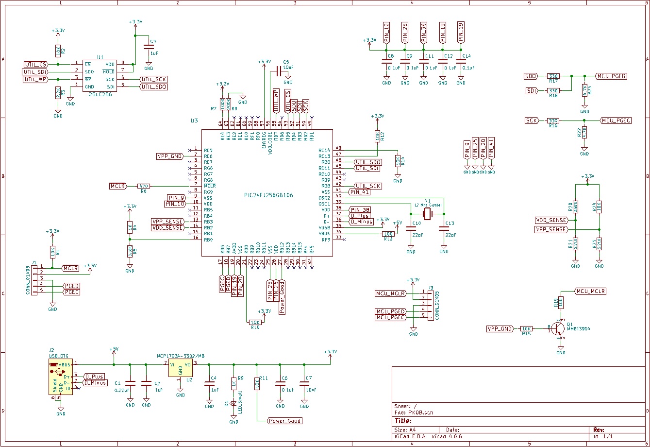
I have a question, I was surfing about the PICkit 3 and found this blog which is a nice job doing DIY PICkit 3 clone. Considering the schematic diagram, for the 3.3V regulator circuit, there are 2 ceramic capacitors on the input and 3 on the output. My question now, is if they are on the same line, why not to use one ?

putting capacitors is still a not clear area for me, even how and when to use inductors.

I know that resistors are to limit the current on series configuration and divide voltage with adjusting the branch current with parallel connection.

But capacitors and inductors are not so clear. Yes capacitors are used in parallel for decoupling purposes, I have read about them here:
What Are Decoupling Capacitors?

Coupling capacitors for blocking DC and passing AC, but didn't do practical experiments about that.

pkob.jpg


Inductors, I have a main idea about them is that they increase current in series, not sure what they do in parallel connection.
--- Updated ---

Close but not quite there yet!

Connect the address pins A0, A1 and A2 of the PCF8575 like you wored them on U5. At the moment they are permanently pulled high and the switches do nothing.

VEE needs to go to the wiper of RP1 and doesn't need a series resistor. RP1 must however be connected between GND and 5V. The idea is that adjusting RP1 will allow VEE to go between 0V and 5V.

Brian.

oh yeah .. I should have been not fully thinking what I'm doing ! serious mistakes !

did them ..

Schematic_pic16f877a_dev_board_2020-12-16_09-28-18.png


what you think of the switches at the power section ? i know there could be other ways to do it. II have to check some PCB designs or projects to learn more about main input management.
 
Last edited:

You still have the address lines on the PCF8575 wrong. Each line should have a resistor to 5V and a switch to GND. They are logic level inputs but draw almost no current so if the switch is open the address line is pulled to 5V (logic high) and if the switch is closed if connects it to GND (logic low).

The VEE connection to the LCD is now correct.

The power switching isn't quite right. You are aiming to get one voltage out from two possible sources so think of the switches being the other way around. Remember a change-over switch gives you two alternative connection routes through it, it isn't just two on/off switches linked together.

Seriously - do not even consider making anything like that PICKIT3 clone. It only has half the functionality of a real one and would only work with some PIC devices, it could damage others.

The idea behind capacitors close to the power inputs of devices is that they are a nearby source of power when the device draws a pulse of current. Do not underestimate the effect of even a few cm of wiring or copper track. It isn't simply that a voltage drop is caused by the resistance of the wiring (Ohms Law) because the resistance might actually be very small, inductance plays a large part as well. Inductance limits the speed at which current changes can flow though a conductor so when a device draws pulses of current, as most do, the voltage at one end of the track might be stable but at the other end it might jump up and down. A capacitor placed physically close to the device act like a reservoir of power, it fills up at its own pace but can release energy exactly where it is needed and very rapidly.

Brian.
 
You still have the address lines on the PCF8575 wrong. Each line should have a resistor to 5V and a switch to GND. They are logic level inputs but draw almost no current so if the switch is open the address line is pulled to 5V (logic high) and if the switch is closed if connects it to GND (logic low).
omg what I'm thinking ! I got back to the design, it's a mess. But I corrected it.


The power switching isn't quite right. You are aiming to get one voltage out from two possible sources so think of the switches being the other way around. Remember a change-over switch gives you two alternative connection routes through it, it isn't just two on/off switches linked together.

OK, what to do in this case ? but you got my idea, I put one main switch for main ON/OFF function and one for selecting between USB or jack input voltage source.

I used these DPDT switches, and chose the routes I want, and left the unwanted unconnected. How about that ? I even thought leaving the unconnected ones isn't very clever, but I was searching for switches yesterday, found rocker switches, SPDT and other types, found these like somewhat would give me 2 input and 4 output. Where I want 2 input and 2 output.

What you suggest me in regard of switches ?

Seriously - do not even consider making anything like that PICKIT3 clone. It only has half the functionality of a real one and would only work with some PIC devices, it could damage others.

OK, thought it's a remarkable work, but ok, it's good for DIY personal project.

Still my questions about the schematic of the project, I want to know why there are 2 caps on the input side of the
3.3V regulator and 3 on the output side ?

A second thought, actually I'm considering like this schematic, how would I know which caps are electrolytic and which are ceramic ?

so for the input side as there are 2 caps, I would assume 1 is ceramic and 1 is electrolytic.
the output would have the same assumption but there still one extra capacitor.


The idea behind capacitors close to the power inputs of devices is that they are a nearby source of power when the device draws a pulse of current. Do not underestimate the effect of even a few cm of wiring or copper track. It isn't simply that a voltage drop is caused by the resistance of the wiring (Ohms Law) because the resistance might actually be very small,
Yep got this part of voltage backup to the IC as they should be near as possible.

inductance plays a large part as well. Inductance limits the speed at which current changes can flow though a conductor so when a device draws pulses of current, as most do, the voltage at one end of the track might be stable but at the other end it might jump up and down. A capacitor placed physically close to the device act like a reservoir of power, it fills up at its own pace but can release energy exactly where it is needed and very rapidly.

Brian.

oh wow I just imagined the how this is a rule in almost all industrial/commercial PCBs, as mounting caps near to ICs, as I've always wondered why there are there. But also there would a lot that have other purposes.

But an important key point here, is that I don't have a profound practical experience in actual electronic systems design; like, choosing the parts to use or also designing a whole board for specific purpose. Easy example would be like, if I'm asked to design the Arduino uno board from scratch, then I wouldn't have a clue of how to design it, what resistors to choose, what caps, ICs ... etc. So I have to follow any design to get the main ideas of the design.

another thing is that I'm not interested in PCB design actually, all I have is dev boards and modules I buy from Aliexpress and that's it.

anyway, I enjoy a bit of learning every time

but when it comes to when I want to do a design, then knowledge comes in hand :)

thanks Mr Brian for all support and information, I really appreciate it !
 

Still my questions about the schematic of the project, I want to know why there are 2 caps on the input side of the
3.3V regulator and 3 on the output side ?
A schematic is just a diagram of how the components connect to each other, it doesn't show their physical location with respect to each other. The capacitors would electrically be in parallel but on the board they would be spaced close to the ICs as explained earlier.

There are no fixed rules about the type of capacitors, ceramic are usually the best but they can be big and expensive beyond a few uF in value. In general, values of 1uF or lower will be ceramic or plastic based and ones above 1uF will be electrolytic.

Brian.
ok yeah, so if in the diagram it's not specified by the symbol of whether the capacitor is electrolytic or ceramic then I would assume by their values. Good to know that.

so what about the power switches ? despite their type of 2 in routes and 4 out.

is my connection in general right ? I'm searching for 2 in and 2 out switches.
 

No, you only need a change-over switch. That is one where the moving contact touches one or the other opposite contacts. (as in your schematic)
Feed USB power to one fixed contact and 5V to the other, the moving contact will then select one or the other depending on the switch position.
For turning the power on or off, you can use a single pole switch or a change-over switch with one fixed contact unused.


Brian.
 

Regarding bypass capacitors, sometimes you WILL see two that are physically close together but one is generally of larger value (say 10uF) and the other of a smaller value (say 0.1uF). They are serving two separate purposes.
The larger value capacitor will smooth out slower voltage changes. For example as power to devices switch on and off or you are getting rid of AC ripple that is still there after the regulator.
The lower value capacitor will smooth out the high frequency switching transients that occur on the power supply lines. These can be in the 10's of MHz range.
Susan
 
This is my today's update:

Schematic_pic16f877a_dev_board_2020-12-17_19-04-10.png


Hope power section is ok. Is there anything I should know for improvement, some ways used in power circuits, is this circuit at the standard level and how to search for some premium stuff used in power circuits ?
 

Looking much better - well done.

Although it isn't wrong, I would predict you will still have power line problems. There are two issues that should be easy to resolve but I will leave you to work out the solution - it is good to learn!

1. D1 will drop some voltage across it. For a normal silicon diode it will be around 0.7V and for a Schottky diode it will be around 0.5V. That may not sound like much but from a 5V supply it may drop the voltage to 4.3V or 4.5V, below what some devices will work at. See if you can work out how to avoid the voltage drop by connecting the switches differently.

2. In the same area, linear voltage regulators like the AMS1117 need some extra voltage at their inputs to work properly. If you put 5V into a 5V regulator it won't have enough 'overhead' for its internal circuits to operate and you will get some lower and maybe unregulated voltage at the output pin. If you check the data sheet for the regulator, the manufacturer recommends no less than 1.3V to allow for drop in the internal circuits. This means to get 5V out you need to put at least 6.3V in. That is probably not an issue from the external power input but consider what reaches the input pin when the USB power source is being used. Again, this is fairly easy to work around if you think about it.

Brian.
 
I cloned the design and did another version with changing the LEDs section because I think it's very important in the beginning of the course that the student can learn a lot of things in this section.

First, this section would be I guess a lot more complicated to start with.

I'm running the LEDs, 7-segments and IR sensors with I2C chips; MAX7219, PCF8575 and PCF8574.
MAX7219 for 7-segments
PCF8575 for LEDs
PCF8574 for IR sensors

Sheet_1.png
 

Hint:
20201219_150324a.jpg


I didn't show the capacitors but they are needed. With the same switches wired this way, either both regulators are fed from the external power through D1 (top input line) or the 5V comes directly from the USB socket and the 3.3V is regulated from the USB voltage (bottom input line). The USB socket input (USBI) should always be 5V if fed from a proper USB host but beware that some phone chargers are either unregulated or produce much higher voltage so please avoid using them.

Brian.
 
Hint:
View attachment 166484

I didn't show the capacitors but they are needed. With the same switches wired this way, either both regulators are fed from the external power through D1 (top input line) or the 5V comes directly from the USB socket and the 3.3V is regulated from the USB voltage (bottom input line). The USB socket input (USBI) should always be 5V if fed from a proper USB host but beware that some phone chargers are either unregulated or produce much higher voltage so please avoid using them.

Brian.

that's not a hint, it's the complete solution :) it took me some time to get the idea. really clever wiring.

Sheet_1.png


power circuit is very important and the most difficult one in this design.

doing this design in actual PCB would cost more than doing a shorter version
this design has a lot of examples onboard, and projects too
the most important project is the traffic system that's why I used 12 LEDs and 4 IR sensors

but still I don't have that clear plan of how to design a course in microcontrollers
I've been 7 years in training, 3 in microcontroller course
3 years is considerable and I don't want to underestimate my experience in training this course
but still, I need more experience in measuring the capacity of knowledge I can deliver ..

the most unclear point me is that I don't have a wide range of experience to measure how students get me and understand what I say in every lab/lecture, I still need more experience/knowledge to grasp the measure of the whole situation including my skills, equipment, level of students' knowledge ... etc.

my ability to measure the situation is the key that would tell me what board I need, what to include, what not to include, what's necessary, ... etc.

not to forget for almost %95 have no experience in programming and microcontrollers in general

but eventually, I think this design is a bit too much for a basic course, I may do a smaller one considering the estimated cost of doing one


also, I ordered the maintenance parts for the old board from Aliexpress, so modifying the old board, then it could serve us, and keep going in the lab
 

hello
I am new member here just three days a go . i have more than 10 years experience programming and design . PIC MUC and Atmega MUC and i am using the two compilers CCS.c compiler and Atmel studio version 6 . regarding " the measure of the whole situation including my skills, equipment, level of students' knowledge ... etc."
the measure of good design is good performance with low cost
 
the measure of good design is good performance with low cost
You're right, I'm not planning to do all that for a simple course, it uses I2C chips and SPI .. etc. A bit complicated for starting the course.

But my plan is for the future when I get to a level in the course where I can start the course teaching I2C, SPI and write some modules libraries. That sounds nice, but considering teaching this stuff in one semester could be too much.

But in reality, I may do a simple board with several LEDs, 4 push buttons, LCD1602, some sensors and that's it, more than enough for one semester.
 

Status
Not open for further replies.

Similar threads

Part and Inventory Search

Welcome to EDABoard.com

Sponsor

Back
Top