Continue to Site

Welcome to EDAboard.com

Welcome to our site! EDAboard.com is an international Electronics Discussion Forum focused on EDA software, circuits, schematics, books, theory, papers, asic, pld, 8051, DSP, Network, RF, Analog Design, PCB, Service Manuals... and a whole lot more! To participate you need to register. Registration is free. Click here to register now.

[SOLVED] How to include a modification in a PIC dev board with PIC16F877A for OVP ?

Status
Not open for further replies.

eagle1109

Full Member level 6
Full Member level 6
Joined
Nov 20, 2014
Messages
393
Helped
4
Reputation
10
Reaction score
7
Trophy points
1,298
Location
Saudi Arabia
Activity points
5,956
Hello,


I work in microcontrollers course in diploma college and I've been training this course for like 2 years now.


I faced different problems with our dev boards because they are basic for voltage input there's only a diode, maybe it's a Zener but I don't think it provides much protection for the components because we already lost several PICkits + PIC16F877As.


I don't want to still loosing PICkits so often. I want to modify the dev board with anything that provides upto like 5.5V max.


I think there are different ways to do it:

1. use lm7805

2. search for dedicated OVP chips, I did a quick search and found one that could be interesting to me which is this one:


I think it's easy to include in the board with some modifications. external connections would be ok as long as we protect our stuff from trainees missing adjusting the variable power supply.


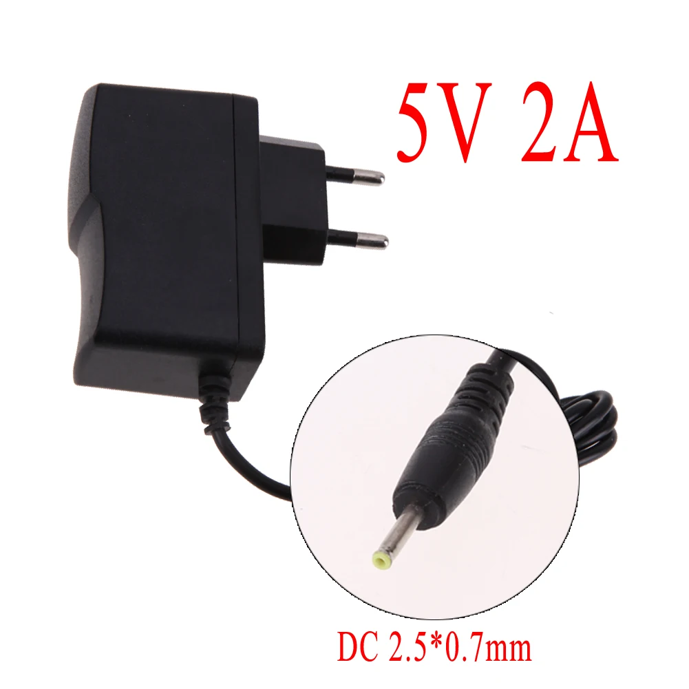
I thought of other solutions, which is to buy a constant 5V adapter, I have one that is 5V/2A, but actually that PICkit didn't catch the 5V ! I don't know why it had to be supplied from the bench variable PSU.
HTB1Y9v3QVXXXXb9XXXXq6xXFXXXb.jpg


This is our dev board and I'm sketching the power input area with yellow circle.

Copy.png
 

What are you currently using as a power supply? What is the current drawn by your development boards
A couple of points to note:
- 7805 devices need a significantly higher input voltage than the 5V output but can also get hot as the current increases (they dissipate the voltage drop as heat so the voltage drop times the current can get to a reasonable figure)
- depending on the input voltage, look for a LDO regulator or buck converter instead
- adapters of the type you show can have a lot of noise on the supply from the switch-mode circuit. You really need to make sure that your board has a lot of bypass capacitors on it, especially around the MCU (and I must admit that I can't quickly see any in your photo)
Susan
 
I agree with Susan, unless there are other components on the other side of the board I would expect it to be unreliable.
I also can't see much point in an opto-isolated relay as both provide isolation anyway.
The relay doesn't appear to have a diode across its coil so it might spike unwanted voltages on to the supply rails.
What is the purpose of the potentiometer (top of the picture) any why is it used with PWM?

At first glance it looks a beautifully laid out but seriously badly designed board.

Brian.
 
What are you currently using as a power supply? What is the current drawn by your development boards

different models like this one:

511RYOHL1bL._SX385_.jpg


the 5V/2A worked but I think when the mcu is programmed with a code that use a lot of current like driving all leds on PORTC high/low, that the PICkit won't respond to the board even actually the PICkit put the mcu in reset mode !

I don't know when I tried the 5V adapter didn't work ! the IPE didn't catch the proper voltage even I lowered the Vcc from the power options.

but in my home with my simple bread board setup using PIC18s it's working with no problems.

A couple of points to note:
- 7805 devices need a significantly higher input voltage than the 5V output but can also get hot as the current increases (they dissipate the voltage drop as heat so the voltage drop times the current can get to a reasonable figure)

yeah ok so it's not the best option I guess, even the board I think won't draw much current more than 1A where lm7805 has 1.5A max o/p current.
yeah maybe at 1A, it could get too hot. so there are much more better options now than the lm7805

but actually there are a lot of stock lm7805s in our warehouse but are used for simple dc power supplies in early electronics workshop courses. but I can take like 20 lm7805 that should serve my mcu course, the lab has 20 PIC dev boards max.

- depending on the input voltage, look for a LDO regulator or buck converter instead
I learned that LDOs are the role now when it comes to voltage regulators. so my question now is lm7805 considered to be old technology and obsolete ?

- adapters of the type you show can have a lot of noise on the supply from the switch-mode circuit. You really need to make sure that your board has a lot of bypass capacitors on it, especially around the MCU (and I must admit that I can't quickly see any in your photo)

I have the schematic diagram for this dev board but a problem is that it's not so clear.

unless there are other components on the other side of the board I would expect it to be unreliable.

you mean connecting external components like sensors, servo motors, .. etc. ?

I also can't see much point in an opto-isolated relay as both provide isolation anyway.

what is the 2nd element that provide isolation ?

The relay doesn't appear to have a diode across its coil so it might spike unwanted voltages on to the supply rails.
yes there's no diode. is that the reason to have an opto-isolator ? and which is best ? a diode or an opto-isolator ?

What is the purpose of the potentiometer (top of the picture) any why is it used with PWM?
going back to the schematic, I think yes it's for variable PWM.

At first glance it looks a beautifully laid out but seriously badly designed board.
yeah, it's our first attempt in college, not my design, it's from one of our colleagues, that he actually helped me a lot with this design.
before i was doing mcu experiments on breadboards which was consuming a lot of lab time, that the lab time is 1:30 hr and most the time there left like 15-20 mins for programming which is really not enough.

so i told our colleague and he started this board design, I really have no idea at that time of how to design one.

now, facing some problems dealing with this board, I learned some stuff, and things to do in order to modify the board and get it at least to serve the course; solving the voltage problems would be enough.


but also there are strange problems I got in this board, the push buttons are connected to PORTD and are pull-down configuration, so the input Vcc is 5V and when I press a button, I get 6V at the input pin !! I don't know how that happens.


----------------------------------------------------------------------------------
this is the schematic:
مخطط كرت معمل المعالجات.jpg

--- Updated ---

This is also pin arrangement table:

pin_arrangement.png
 
Last edited:
Its difficult to read the labels on the signals but there are certainly some serious errors in the schematic.

1. You absolutely MUST add decoupling capacitors across the supply. C3 alone is not enough and we can't see it anyway. Use several combinations of 100nF ceramic and 10uF electrolytics in parallel, including one pair as close as possible across the VSS and VDD pins of the MCU. Without the capacitors there will be a lot of noise on the supply lines and a poor return path for the internal oscillator currents.

2. Add a diode across the relay coil with its cathode end towards VCC. This is because when the coil turns off it, the collapsing magnetic field creates a high voltage that could damage the driver transistor and possibly other components too. The diode will not conduct except for when it is absorbing the voltage spike.

3. R32 in the open collector section will burn out if the pins are linked and it is set to low resistance. Open collector should not have a current source from VCC at all but if you wire it like it is, you must at least make sure the current is limited. Think what would happen if you set R32 to zero resistance (turned all the way to the end) and you made the transistor conduct, it would short out the supply lines.

4. You have no protection against an MCU pin being driven low and closing one of the push buttons to VCC. Connecting supply directly to a pin driven low will likely burn out the internal driver transistors.

5. There is absolutely no point in using an opto-coupler in that way. The idea behind them is that the input side is isolated from the output side so feeding them from the same supply lines is pointless. Either use the transistor and the relay -or- use the optocoupler but not both at the same time.


Brian.
 
Its difficult to read the labels on the signals but there are certainly some serious errors in the schematic.
Yeah, this is what I got from our colleague. He just sent me this.

OK, so the first obvious solution is to take the components out and throw these boards, design a new better one and that's it! But there are some complications here:
1. These lab boards are in lab for like 2 years ago that time the money was good in our department.
2. Now money is a problem and I'm now facing boards problems and can't do simple laboratory experiments; like, led blinking and read input pins
3. I even asked for some materials; like, 22awg cables, banana connectors, better header pins, terminal connectors and rubber feet to at least improve the current hardware we have in the lab and these materials only cost like $120 from aliexpress and also having problems getting funded to purchase them.
4. Doing a new board would have even more financial problems.

The board in the picture is most board that has most the components soldered, the rest just have leds, push buttons and lcd, because I can't go to more advanced experiments because trainees have like near zero experience in programming with C.

1. You absolutely MUST add decoupling capacitors across the supply. C3 alone is not enough and we can't see it anyway. Use several combinations of 100nF ceramic and 10uF electrolytics in parallel, including one pair as close as possible across the VSS and VDD pins of the MCU. Without the capacitors there will be a lot of noise on the supply lines and a poor return path for the internal oscillator currents.

2. Add a diode across the relay coil with its cathode end towards VCC. This is because when the coil turns off it, the collapsing magnetic field creates a high voltage that could damage the driver transistor and possibly other components too. The diode will not conduct except for when it is absorbing the voltage spike.

3. R32 in the open collector section will burn out if the pins are linked and it is set to low resistance. Open collector should not have a current source from VCC at all but if you wire it like it is, you must at least make sure the current is limited. Think what would happen if you set R32 to zero resistance (turned all the way to the end) and you made the transistor conduct, it would short out the supply lines.

4. You have no protection against an MCU pin being driven low and closing one of the push buttons to VCC. Connecting supply directly to a pin driven low will likely burn out the internal driver transistors.

5. There is absolutely no point in using an opto-coupler in that way. The idea behind them is that the input side is isolated from the output side so feeding them from the same supply lines is pointless. Either use the transistor and the relay -or- use the optocoupler but not both at the same time.

These consideration points should be taken into accounts in the new design for God's will and thank you so much for clearing out these important design tips. But now I can't dream of one because they say no money :) so I have to deal with what is in the lab right now and do the improvements of cables, connectors .. etc. at least to get the boards connect to the PC.
 
Last edited:

You have mentioned the PicKit - can you explain how you are using that wth this board?
With a board like this you should be powering it with the external PSU and using the PicKit ONLY for programming. There is not way that the PicKit can be used to provide power to the board at any time so you need to make sure that the IDE that is connected to the PicKit is set to use target power only.
Susan
 
I would suggest at least adding a diode and extra capacitors as suggested. You can wire them on the back of the board between the existing component pins, not ideal but it works.

Brian.
 
You have mentioned the PicKit - can you explain how you are using that wth this board?
With a board like this you should be powering it with the external PSU and using the PicKit ONLY for programming. There is not way that the PicKit can be used to provide power to the board at any time so you need to make sure that the IDE that is connected to the PicKit is set to use target power only.
Susan
yes you're right the board has no lines for PICkit power. the power is external all the time and I'm unchecking power from target tool.


I would suggest at least adding a diode and extra capacitors as suggested. You can wire them on the back of the board between the existing component pins, not ideal but it works.

Brian.

the diode can be routed somehow but the capacitors are a bit difficult.

you mentioned

Use several combinations of 100nF ceramic and 10uF electrolytics in parallel
how to do that ?

should I solder two 100nF across main power lines ?
--- Updated ---

I took pictures for how we operate these boards in our lab.

20201207_102218_resize_89.jpg


20201207_103218_resize_70.jpg


20201207_102516_resize_55.jpg


20201207_102457_resize_0.jpg
 

Attachments

  • 20201207_102218_resize_89.jpg
    20201207_102218_resize_89.jpg
    325.8 KB · Views: 260
Last edited:

I can see C3 isn't fitted at all, its a wonder it ever works!

Fit 10uF in C3 position.
Flip the board over and solder 100nF capacitors with short wires directly across pins 11 & 12 and across pins 31 & 32. You can use the solder pads of the socket to connect to.

Similarly, flip the board over and solder a diode directly across the solder pads of the relay coil. A small signal diode like a 1N914/1N4148 will do.

Something puzzles me: I have never seen a PIC16F877A in a skinnydip package and none of the data sheets show it either. Are you sure it really is that device or is the photograph resized to make it look narrower?

Brian.
 
I can see C3 isn't fitted at all, its a wonder it ever works!

I don't know actually what is the role of C3 ?! It's apparently an electrolytic capacitor across power lines and then we have 100nF caps also across Vdd and Vss which also the power lines.

Fit 10uF in C3 position.
Flip the board over and solder 100nF capacitors with short wires directly across pins 11 & 12 and across pins 31 & 32. You can use the solder pads of the socket to connect to.

ok, got that, yes the socket pads would be more safer approach.

Similarly, flip the board over and solder a diode directly across the solder pads of the relay coil. A small signal diode like a 1N914/1N4148 will do.

there are a lot of diodes in the warehouse, the diode install should be easy I hope.

Something puzzles me: I have never seen a PIC16F877A in a skinnydip package and none of the data sheets show it either. Are you sure it really is that device or is the photograph resized to make it look narrower?
Yep I resized the photos


thank you so much for the support, you don't know how much I enjoy reading your replies, it contains a lot experience with the provided information, really enlightening !
 

C3 and the others across VSS and VDD are what we call 'decoupling' capacitors. I will explain why they are so important:

The current drawn by the MCU appears to be quite low, just a few mA and that is what a test meter would show. However, it isn't constant, there are thousands of transistors in the MCU and each time one turns on or off it draws a spike of current. The spike is caused by the need to charge up or discharge the internal capacitance of the circuits and in some cases many (possibly hundreds) of transistors will switch simultaneously. As they do, their combined current for a few nS can be quite high. A meter wouldn't have time to react and would only show the average value, not the peaks. Because of the resistance and inductance of the wiring back to the power supply, a spike in current will cause a significant drop in voltage at the MCU, it may be several volts. Again because a meter can only react slowly it doesn't see the brief drops but the rest of the circuitry inside the MCU certainly will.

It could be fixed by mounting the MCU and power supply very close together, maybe lass than 10mm apart but that obviously isn't a practical solution. Instead we mount decoupling capacitors as close as possible to the device drawing the spikes of current. The capacitors store charge from the supply and release it when the voltage starts to drop and being very close to the load they do it without the losses of the supply wiring. Think of them as little rechargeable batteries mounted right where their power is needed. That's why I recommended them wired directly across the VSS and VDD pins of the MCU with short wiring length.

At first it might seem sensible to use a capacitor with a large value so it would have more power stored and therefore work better. In a perfect World that is exactly what we would do but unfortunately most capacitors, especially electrolytic ones, while being good at storing lots of charge are not so good at releasing it rapidly. Ceramic capacitors are very good at releasing charge rapidly but are physically big when large values are needed. Using both types in parallel gives the ability to store and release large amounts of charge at high speed. Typically 10uF electrolytic and 100nF ceramic are wired across the supply and so as one becomes less good at high speeds, the other takes over and becomes more effective.

Brian.
 
C3 and the others across VSS and VDD are what we call 'decoupling' capacitors.

Yeah you told me before in an earlier post that they serve like balancing the currents drawn by the mcu so there won't be any voltage fluctuations across power rails.

Thank you so much for the detailed explanation. I certainly may not grasp the full understanding but I got some main ideas of the different scenarios with the problem of internal current spikes and their effect of supply voltage.

I will explain why they are so important:

The current drawn by the MCU appears to be quite low, just a few mA and that is what a test meter would show. However, it isn't constant, there are thousands of transistors in the MCU and each time one turns on or off it draws a spike of current. The spike is caused by the need to charge up or discharge the internal capacitance of the circuits and in some cases many (possibly hundreds) of transistors will switch simultaneously. As they do, their combined current for a few nS can be quite high. A meter wouldn't have time to react and would only show the average value, not the peaks. Because of the resistance and inductance of the wiring back to the power supply, a spike in current will cause a significant drop in voltage at the MCU, it may be several volts. Again because a meter can only react slowly it doesn't see the brief drops but the rest of the circuitry inside the MCU certainly will.

so without decoupling capacitors, could I connect and oscilloscope between Vdd and Vss, and then I might observe the fluctuations on the Vdd pin ?

It could be fixed by mounting the MCU and power supply very close together, maybe lass than 10mm apart but that obviously isn't a practical solution. Instead we mount decoupling capacitors as close as possible to the device drawing the spikes of current. The capacitors store charge from the supply and release it when the voltage starts to drop and being very close to the load they do it without the losses of the supply wiring. Think of them as little rechargeable batteries mounted right where their power is needed. That's why I recommended them wired directly across the VSS and VDD pins of the MCU with short wiring length.
ok got that

At first it might seem sensible to use a capacitor with a large value so it would have more power stored and therefore work better. In a perfect World that is exactly what we would do but unfortunately most capacitors, especially electrolytic ones, while being good at storing lots of charge are not so good at releasing it rapidly. Ceramic capacitors are very good at releasing charge rapidly but are physically big when large values are needed. Using both types in parallel gives the ability to store and release large amounts of charge at high speed. Typically 10uF electrolytic and 100nF ceramic are wired across the supply and so as one becomes less good at high speeds, the other takes over and becomes more effective.

Brian.

oh ok, I also wonder sometimes when I run different PCB models, that there are different types of non-electrolytic capacitors, the blue ones, the dark red ones, yellow .. etc. They called polymer, ceramic, Polyester .. etc.

types-of-capacitors.jpg


This picture is really good, at least it categorized the different types of capacitros, but I think these are not all types, but most ones.
I understood one time, that the difference is related to voltage and frequency ratings, as they are the most important rules to choose which capacitor fit the application circuit.


Also I got the idea of using and electrolytic + ceramic, to provide the best of the two worlds. As the electrolytic would work as a bulk main reservoir and smoothing element and the ceramic would work as fast duty voltage balancing to the mcu.
 

so without decoupling capacitors, could I connect and oscilloscope between Vdd and Vss, and then I might observe the fluctuations on the Vdd pin ?
Quite likely but beware of the scope probes themselves introducing noise as well.

The different of capacitors have different properties. The voltage rating is how much they can reliably hold across them, the capacitance is how much charge they can hold and the substance they are made of gives them other special properties. Some are compact for their value, some are stable over wide temperature ranges and some are capable of passing high currents without damage. If you look up data on capacitors you will see things like temperature coefficients, ripple currents and HF impedance mentioned, the circuit designer picks the type best suiting the application.


Brian.
 

FYI there is a parallel discussion occurring at https://www.microchip.com/forums/m1159671.aspx but that seems to be more about designing a new board than getting this board to remain useful.
Just cross-referencing these so the OP doesn't get too many overlapping and/or contradictory suggestions.
Susan
Yes, but mostly these two forums are the most common forums for me when it comes to electronics and best ones for me too.

I get really entertained following my posts everyday.
actually the timing of the threads is different, when I thought about the pcb design i posted in microchip forum, as i hope they would provide me with a ready design for the pic, but I guess I have to work that by myself, so now I have to continue my discussion there and post my design on easyada to get the recommendations and tips from forums members.
 

hi,

I'm working on a dev board design. I also bought some mod parts for the old dev board.

putting the new design in halt condition in case the department agreed to proceed financing the schematic

**broken link removed**

I'm still working on the LCDs now, hope you like it in general :)
 

Some observations:
1. C6 & C7 values are FAR too high, something like 22pF would be more appropriate.
2. add capacitors (about 1uF) between the input pins of the regulators and their GND pins. Physically they should be a close to the regulator as possible.
3. I would suggest adding a switch from the MCLR pin to ground to allow it to be manually reset.
4. Be careful connecting 'VCC' directly to 'V_USB'. VCC has to be higher than 5V for the AMS1117-5.0 to work but connecting it directly to the USB socket could damage anything plugged in to it.
5. my choice of value for R1 would be 100 Ohms, it should work with 1K but it would be safer to use a lower value so the logic low level is nearer 0V when a switch is closed.

Brian.
 
Some observations:
1. C6 & C7 values are FAR too high, something like 22pF would be more appropriate.
yep I did that just now.

2. add capacitors (about 1uF) between the input pins of the regulators and their GND pins. Physically they should be a close to the regulator as possible.

I added electrolytic capacitor C1 = 47uF, I thought it'd enough. Do you mean another ceramic caps too along with C1 ?


3. I would suggest adding a switch from the MCLR pin to ground to allow it to be manually reset.

Thanks for the tip ! Totally forgot about that :)

4. Be careful connecting 'VCC' directly to 'V_USB'. VCC has to be higher than 5V for the AMS1117-5.0 to work but connecting it directly to the USB socket could damage anything plugged in to it.

Did that too, wow, I'm just rushing through the design without much deep experience, but thanks for the support. Didn't know what VCC could really be something more than 5V.

But I'm still considering the nice options for powering the board. I included a screw 2-pin terminal connector and a USB until now. But also thinking about a power jack because the goal is to use 9V adapters from Aliexpress.

5. my choice of value for R1 would be 100 Ohms, it should work with 1K but it would be safer to use a lower value so the logic low level is nearer 0V when a switch is closed.

Brian.

just did that, I actually followed this tutorial:


1607611075382.png


Embed With Elliot: Debounce Your Noisy Buttons, Part I

This is my last design:

Schematic_pic16f877a_dev_board_2020-12-10_17-36-20.png


I also followed their approach in debouncing using an inverter.
 

hi,

this is my recent work. after putting much modules and component. I started to think it's a bit too much for the purpose of the course.
the course is actually a scratch beginner in microcontrollers.

mostly LEDs, LCD1602, several push buttons, LM35, 2digit 7-seg and a rely are more than enough for the course
and most of the stuff has to be put in female sockets for maintenance

I think the current one is ok, just need the mods and upgrade material I already ordered from aliexpress and all good

anyway here's my latest work on the design:

Schematic_pic16f877a_dev_board_2020-12-12_00-30-02.png
 

Status
Not open for further replies.

Similar threads

Part and Inventory Search

Welcome to EDABoard.com

Sponsor

Back
Top