Continue to Site

Welcome to EDAboard.com

Welcome to our site! EDAboard.com is an international Electronics Discussion Forum focused on EDA software, circuits, schematics, books, theory, papers, asic, pld, 8051, DSP, Network, RF, Analog Design, PCB, Service Manuals... and a whole lot more! To participate you need to register. Registration is free. Click here to register now.

how to find switching losses in LTSpice

Praveen_Raj

Newbie level 5
Newbie level 5
Joined
Nov 9, 2024
Messages
9
Helped
0
Reputation
0
Reaction score
0
Trophy points
1
Activity points
57
I'm trying compare the efficiency of an inverter (power R1 / input Power) at different switching frequencies to understand switching losses, but im getting the same efficiency of 95.4% when Fs = 10 and Fs= 100k.
I'm using Mosfets with Vds = 600V

Can someone please help me understand why this is happening....
1731218895012.png
 
You are operating AOD280A60 far above useful current range and get mainly conduction losses.
--- Updated ---

For realistic switching simulation, you also need to set feasible gate drive conditions.
 
You are operating AOD280A60 far above useful current range and get mainly conduction losses.
--- Updated ---

For realistic switching simulation, you also need to set feasible gate drive conditions.
I have made it such tha Id only goes upto 9A as per datasheet,
now for switching freq of 10hz im getting an efficiency 99.49 and of and 100khz im getting an efficiency of 99.42

1731235242241.png

and if u dont mind could you tell me what are the feasible gate drive conditions would be.
thank you
 
Sorry but its not really possible in LTspice to get switching losses accurately. The MOSFET junction capacitances are not modelled properly over the voltage range. Also, the stray inductances in the drive circuit, etc, are not modelled realistically.
 
Sorry but its not really possible in LTspice to get switching losses accurately. The MOSFET junction capacitances are not modelled properly over the voltage range. Also, the stray inductances in the drive circuit, etc, are not modelled realistically.
Don't agree. It completely depends on model quality. Some vendor models have accurate junction capacitance and also package inductance.
 
If im not wrong, im getting...
power dissipated by mosfet without llc at low freq in mW
power dissipated by mosfet without llc at high freq in W

power dissipated by mosfet with llc at high freq (resonant freq) in mW
(the above checks out)
and some how im getting lower power with llc at freq higher than resonant freq
 
If you post your .asc file (and any required symbol/library files) we can probably help a lot faster.
--- Updated ---

Sorry but its not really possible in LTspice to get switching losses accurately. The MOSFET junction capacitances are not modelled properly over the voltage range. Also, the stray inductances in the drive circuit, etc, are not modelled realistically.
There are a lot of reasons simulated losses might be inaccurate, but usually manufacturer models do a very good job of replicating device capacitance. At least that's what I've seen from Vishay, Infineon, and STM. Not sure about AO, but would expect the same.
 
Ah yess, sorry

Apparently i can't upload straight .asc file, so imma upload em in a compressed folder
 

Attachments

  • Inverter.zip
    1.8 KB · Views: 14
can someone please suggest me what to do, or who to ask, like this might not seem much, but it's a part of my final year project, i need to get this thing done asap
 
"Wallplug" efficiency is easy. Two frequencies, same load on same power train. The difference is all in the switching.

In figuring efficiency terms I think it's cleaner to work with the loss terms (inefficiencies) that are its elements. There might be competing mechanisms that obscure "what to improve" if you look only at the bottom line, converter-level Pout/Pin.
 
I don't see anything "wrong" with your simulation. A few observations:
1. In the case where the load resistance is very high (near infinity), the only source of loss is due to the FET's Coss charging and discharging. The LTspice model takes about 40nC of charge to change Vds from 0V to 600V. The energy required is that multiplied by the bus voltage, which is 40nC*600V=24uJ. This happens twice per switching period (once for each edge), and for each half bridge, so combined switching loss across all four FETs is 96uJ*Fsw.
2. When the load resistance is lower (like 100-1K), then things get more complicated. As load current increases, overlap switching losses will increase. Overlap switching losses will also depend on switching time, but because your gate drive is so fast it's still very low. Capacitive switching losses on the other hand actually decreases due to the load resistance. This is because much of the energy stored in the capacitances will now be delivered to the load instead of dissipated in the FETs. Overall, you may paradoxically observe that total switching losses is much lower than with no load at all.
3. If you keep reducing Rload, eventually overlap switching losses will start contributing significantly, but by then the total losses will be so high that the device will be dead anyways.

But if your intent is to work on a LLC design, I don't understand what the purpose of this simulation with a simple load resistance actually is. It's not going to be directly comparable to an LLC circuit.

When operating properly (i.e., all FETs turn on with near zero voltage), it is expected that switching loss will be nearly zero, and therefore switching frequency will have no direct impact on efficiency (assuming that as frequency is changed the design of the LLC network also changes to maintain constant output power). That's the main point of the LLC topology.

can someone please suggest me what to do, or who to ask, like this might not seem much, but it's a part of my final year project, i need to get this thing done asap
Maybe state some more specific questions then...
 
I don't see anything "wrong" with your simulation. A few observations:
1. In the case where the load resistance is very high (near infinity), the only source of loss is due to the FET's Coss charging and discharging. The LTspice model takes about 40nC of charge to change Vds from 0V to 600V. The energy required is that multiplied by the bus voltage, which is 40nC*600V=24uJ. This happens twice per switching period (once for each edge), and for each half bridge, so combined switching loss across all four FETs is 96uJ*Fsw.
2. When the load resistance is lower (like 100-1K), then things get more complicated. As load current increases, overlap switching losses will increase. Overlap switching losses will also depend on switching time, but because your gate drive is so fast it's still very low. Capacitive switching losses on the other hand actually decreases due to the load resistance. This is because much of the energy stored in the capacitances will now be delivered to the load instead of dissipated in the FETs. Overall, you may paradoxically observe that total switching losses is much lower than with no load at all.
3. If you keep reducing Rload, eventually overlap switching losses will start contributing significantly, but by then the total losses will be so high that the device will be dead anyways.

But if your intent is to work on a LLC design, I don't understand what the purpose of this simulation with a simple load resistance actually is. It's not going to be directly comparable to an LLC circuit.

When operating properly (i.e., all FETs turn on with near zero voltage), it is expected that switching loss will be nearly zero, and therefore switching frequency will have no direct impact on efficiency (assuming that as frequency is changed the design of the LLC network also changes to maintain constant output power). That's the main point of the LLC topology.


Maybe state some more specific questions then...
Thanks alot for looking into it,
What im trying to find is, when the load R is constant (say 1000), At switching freq = resonant freq of LLC (459kHz), the switching losses is near 0, so id assume we'd get least power dessipated through FET.
but when i increase the switching freq above resonant freq, im getting a lower power dissipation.
The only purpose of this circuit is to realize the soft switching by LLC (Does this circuit not work as i want it to?)
(If my assumption is incorrect here, please let me know).
And again thanks alot of looking into it.
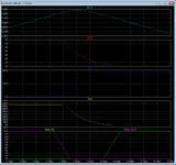
So let's look a little closer at the simulation with the simple load resistance (100 ohms in this case), zoomed in at the moment when V(a) falls and V(b) rises. You can see that during the 150ns dead time, both V(a) and V(b) are pulled to Vbus/2=300V. This is sort of "halfway" to soft switching. But you would never see this sort of waveform in a circuit with a real transformer on the output (like an LLC). Even if you actually built this circuit in real life it likely wouldn't show these waveforms, as it depends on perfect symmetry between all the gate drivers and FETs. But basically this simulation isn't useful for the purpose of investigating an LLC converter.
1731589818730.png

For this simulation, each FET dissipates an average of 5.08W, total losses are 20.32W. Total load power is going to be constant between simulations, so not going to bother mentioning it, just looking at FET losses is enough.

There's a few simple changes I made to make it more "realistic", but without adding a full-blown LLC network on the output:
1. Increased the gate rise/fall times to 50ns (set with the param trf)
2. Added an inductor in parallel with the load resistance (set with the param Lp). This roughly emulates the magnetizing inductance of a transformer, for achieving true soft switching.
3. Added additional capacitance across each FET (set with param Coss_ext). In practice this is often done with soft switching converters to reduce EMI.

First I'll set Coss_ext to 1nF and Lp=10H (so Lp effectively is an open circuit). The same waveforms change to this:
1731591553568.png

Overall not much different, except that V(a) and V(b) take longer to "half-soft-switch" due to the extra capacitance, but the dead time is still long enough that V(a) and V(b) reach nearly 300V before the end of the dead time. The extra capacitance also causes switching losses to increase quite a bit. Each FET now dissipates an average of 10.55W, for a total loss of 42.16W.

Now let's change Lp to 200uH and run it again (making sure to run the simulation long enough for the current in Lp to reach steady state):

1731592118800.png


This is "real" soft switching behavior. V(a) and V(b) transition all the way to 0V and 600V respectively within the dead time. The switching losses are now nearly zero, but conduction losses are increased relative to the previous simulation due to the extra current flowing through Lp. But the overall losses are reduced compared to the previous simulation: each FET dissipates 8.46W, or 33.9W total. You can play with the various parameters (Coss_ext, Lp, td, etc) to see how they effect efficiency/losses. Actually separating switching and conduction losses in such a simulation is actually quite tricky, and would best be done with clever use of .meas statements.

I've attached the .asc file which generated the results above, and a .plt file for setting up the plots.

IMO this simulation is a much more useful starting point for investigating an LLC (also other soft-switched topologies like the PSFB). As you get more familiar with it, you can add on the resonant parts and make it a true LLC.
 

Attachments

  • 1731591868529.png
    1731591868529.png
    58.8 KB · Views: 4
  • Inverter v2.zip
    1.6 KB · Views: 4

LaTeX Commands Quick-Menu:

Similar threads

Part and Inventory Search

Welcome to EDABoard.com

Sponsor

Back
Top