Continue to Site

Welcome to EDAboard.com

Welcome to our site! EDAboard.com is an international Electronics Discussion Forum focused on EDA software, circuits, schematics, books, theory, papers, asic, pld, 8051, DSP, Network, RF, Analog Design, PCB, Service Manuals... and a whole lot more! To participate you need to register. Registration is free. Click here to register now.

Help with spec'ing FETs for 11A @ 26V led driver

Status
Not open for further replies.
Yes I am aware of the 60V breakdown voltage. It was a mistake as I assumed the voltage across the diode would never rise above the max input voltage. Even so at 22 - 27Vin and 26Vled, that is still a maximum of 53V. I don't think this is causing the circuit to fail at these lower input voltages. Also remember, that the circuit works at these low input voltages if the output current is lowered to 5A which equates to Vled of about 23V.
There are 2 diodes in the one package, thus there are 2 diodes in the circuit. Layout is per the schematic. That diode does get warm but there is a massive heat sink that is attached to both FET's and the diode. I may put another diode package in there also. What is the general feeling on paralleling up diodes in this situation?
I am still not sure why the duty cycle goes above 55 or 57%. That should be the maximum but it looks like it goes to 99% before it trips into hiccup mode.
 

I also noticed the current limiting resistors of 0.027 ohms (x2 in parallel) will limit the Nch MOSFET current to peak of 31 amps. This is less then the peak required current at lower supply voltage end of over 35 amps.

The current limit resistors voltage drop also shaves off another 0.4 volts of the already skimpy Nch-MOSFET gate drive voltage at the point where they need the lowest Rds-ON. It is hard to guess what the true Rds-ON is going to be as the gate drive level is right as the point where Rds-ON shoots up from insufficient Vgs drive.

If your inductor can handle 42 amps peak then set current limit resistor to 0.010 ohms.

It is not easy to get a good heat transfer through a FR4 fiberglass board. Fill the pad area with as many vias as you can. Then getting good thermal connection from backside to heat sink is difficult. I would put several screws in the area to get as much tight surface contact as you can.
 
Last edited:

I'll try the resistor change. I'd love to see your calculations too. The pcb is screwed to a heatsink but there is also a huge heatsink clamped to the top of the fets and diode. In total there will be around 14lbs of aluminum that this pcb will be thermally connected to. And then there is the fan on the back!
 

You should build a computer sim so you know what you are dealing with. That is what I did.

You cannot possibly have 90% duty cycle with an 8.2 uH coil as the source current limit sense would truncate the MOSFET cycle at 31 amps peak current with present sense resistors. That would limit conduction to about 50% duty cycle.

It may ramp up a bit further then the 31 amp trip as I am sure there is some filtering on sense input to avoid it tripping at beginning of cycle when MOSFET dumps its Cds charge which creates a short initial current spike. Most is contained within MOSFET, not seen by sense resistor, but any external capacitance, like rectifier diode and PCB stray will show up on sense resistor.

You must have some excess resistance somewhere in the path. Either MOSFET not fully turning on, power supply cannot supply current, or some resistance elsewhere on the PCB.

Get a scope and work your way up the stack from sense resistors, MOSFET drain, to power supply ripple.
 
Last edited:

The only sim software I have is Linear Techs LTspice.
I'd guess that any excess resistance comes from the pcb traces. This proto is only 1oz copper but the widths are designed for 3oz. At the gate of each FET i have a 1N4148W and a 10r resistor in parallel. The gate turn on looks sharp with only a small bit of bounce at turn off. Perhaps I should reduce the 10r resistor to a 2.2r or something.
The other thing I thought of was ripple across the sense resistors. Datasheet calls for a max of 40mV, I haven't looked at this yet.
 

So after a break working on this for a different project, I am back to this design. I have fixed several of the problems and now am left with only one but it is fairly major. In cleaning up and fixing the other issues I now have massive ringing on the drain of the FET's. The waveform here previously wasn't anywhere near this bad so I'm not sure what happened. I'll put a snubber on to help reduce this but any other suggestions? I thought about a 10r resistor on the gate to add a little time for recovery.

Pic of scope screen showing ringing will be added shortly.

EDIT: Ringing is due to light load but the waveform is very nice with more load. On spikes are the problem. Need a scope with higher bandwidth to measure them.
 
Last edited:

I believe I've found the last issue with this design - if anyone is still following, I'll explain.

I'm using two diodes in a paired array and it appears this is the issue. If I lift one of the leads and have just one diode in circuit, all the noise, spikes and instability goes away. As a matched pair of diodes in the same physical package, I wouldn't have thought that this would be an issue.
 
Last edited:

Ok, so after several revisions I am still having units fail after a while. I am now using 4 IRF6646 in parallel and have a snubber circuit. The diode has also been changed to a 100V 20A device with a 900mV drop.
After a while the drivers seem to loose power and current limit between 6 and 7A. Duty cycle shifts to device max where it should be 55%. Temperature does not seem to be the issue as the boards run cool enough and I can heat them up with a hair drier and watch the signals change on a scope. Output specs are maintained.

So any ideas why these things might be failing? I've pulled a couple apart and all components are in spec with regards to value. I've put these parts on known working boards and they continue to work.

This is very discouraging as this is my first design over 200W and finally thought I'd got it right.
 

Ok, so after several revisions I am still having units fail after a while. I am now using 4 IRF6646 in parallel and have a snubber circuit. The diode has also been changed to a 100V 20A device with a 900mV drop.

After a while the drivers seem to loose power and current limit between 6 and 7A. Duty cycle shifts to device max where it should be 55%. Temperature does not seem to be the issue as the boards run cool enough and I can heat them up with a hair drier and watch the signals change on a scope. Output specs are maintained.

So any ideas why these things might be failing? I've pulled a couple apart and all components are in spec with regards to value. I've put these parts on known working boards and they continue to work.

This is very discouraging as this is my first design over 200W and finally thought I'd got it right.

May I say I feel your 'pain'. This might be dangerous but would you consider 'binning' it and trying something different?

I am not sure I should moan about what Maxim is doing to you but at the moment it looks fairly horrible. Not your problems. I really think they should be trying harder or at least demonstrating slightly more knowledge about their IC and the way it might function in their circuits

Do I rubbish it to make myself 'look good'? It seriously is not your fault especially when Maxim are demonstrating less of a clue about things.

Seriously.. If you look on Page 7) of the Data Sheet then there is a graph that shows the circuit delivering 500mA into the diode string and the evaluation board is rated at 1A up to 36V. You are more than pushing things to get 10A @ 26V.

Let's say you expect 50% duty cycle at 80KHz with a 26V input and 26V output using the 'boost' topology with your 8.2uH inductor. The sums do, not or they do, work..

6.25uS on time gives you a peak inductor current of 22.8 Amps. That is setting from 0A to 22.8A from the 26V supply. It will get reset from 22.8A back to 0A through the same voltage. Since you are dealing with 50% sawtooths then the average input/output current will be 1/4 of that or 5.7A.

These are huge ripple currents which will, as you have seen, hammer any input or output capacitors you wish put on the supply itself and hammer the input supply without them.

It's also going to probably 'hurt' the inductor. Ripple current to that level is going to result in large winding and core losses. It might be 'rated peak' for the job as you see it but it might not be happy otherwise.

Some of your other problems might arise from loop compensation issues. On Page 13) of the Data Sheet they make reference to a Right Half Plane Zero when you have continuous inductor current. No.. I think I'll ignore that because it would be too much of a waste of time.. or that will be me being lazy.

As suggested I think the circuit(s) as presented by Maxim is/are meant to be used at much lower power levels and, by following the design notes as presented in order to gain more output power you are going down a blind alley. I also think the Maxim technical support team are doing you no favours by not suggesting that you will be getting yourself in trouble.

Let the 'danger' begin.

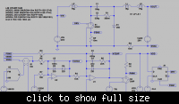
Since you have LTSpice, which is 'nice' have a look at this.


Code:
* C:\LED\cuka.asc
LP VIN N001 75µ
LS VOUT N003 75µ
S1 PSNS N001 DRV 0 MSW
C1 N002 N001 100µ
D1 N002 0 DID
VIN VIN 0 30V
LL N002 N003 15µ
C2 N004 N001 330µ
R1 N002 N004 390m
VLED SSNA VOUT 26V
RS SSNA 0 10m
RP PSNS 0 10m
A1 VDD 0 N012 0 PWM 0 DRV 0 DFLOP Vhigh=15 Vlow=0 Trise=50n Tfall=50n Td=10n
S2 0 PWM VCEAP N013 CMP
R2 VDD PWM 1K
VDD VDD 0 15V
V§CLK N012 0 PULSE(0 15 0 10n 10n 1u 10u)
V§TRI N013 0 PULSE(1 5 500n 9u 1u 0 10u)
XU1 N005 0 VCEAP opamp Aol=100K GBW=10Meg
C3 VCEAP N005 620p
R3 N005 PSNS 1K
R4 N005 VCEAS 10K
C4 N007 N005 3n3
R5 VCEAP N007 22K
D2 N005 VCEAP ZID
XU2 N006 0 VCEAS opamp Aol=100K GBW=10Meg
C5 VCEAS N006 100n
D3 N006 N008 ZID
D4 VCEAS N008 ZID
R6 N006 SSNB 1K
R7 N006 N011 10K
V§IDEM N011 0 1V
E1 SSNA SSNB N010 0 0m
A2 N009 0 0 0 0 0 N010 0 MODULATOR Space=100 Mark=100K
VMOD N009 0 PWL(0 0 100m 0 110m 1)
.model D D
.lib C:\Program Files\LTC\LTspiceIV\lib\cmp\standard.dio
.MODEL MSW SW(RON=10m ROFF=1E9 VT=5)
.MODEL CMP SW(RON=10m ROFF=1E9 VT=0)
.MODEL DID D(RON=10m ROFF=1E9)
.MODEL ZID D(RON=10m ROFF=1E9 VREV=5V)
.tran 0 15m 10m 100n uic
.LIB OPAMP.SUB
K1 LP LS 1
.backanno
.end

Hopefully if you copy the above code and paste it into your text editor then save the file as a .asc LTSpice should recognise and open it for you. Shout if it does not work.

I've added * C:\LED\cuka.asc at the beginning which is where I saved it.

It is a coupled inductor CUK converter and I will not deny that I am 'guessing' at things and it will need some work to qualify and sort it. Depends on whether you wish to invest time in it but, hopefully, the result will be 'nicer' than what you are dealing with at the moment.

As per the links given in..

https://www.edaboard.com/threads/198743/#post838978

I am using average current mode control of the 'primary' switch, S1, to avoid external resonances which may not be controlled. The coupled inductor would/will be designed to place leakage in the output steering ripple to the input. This will be a custom design. I can do that.

U1 controls the 'primary' switch current which, as detailed by Dixon, will be the input current. As he explains in the the application note component, C3, is selected to achieve 'slope matching'. I have not analysed it, done the sums properly. I took a guess at R5/C4, C4 was 'easy' and it worked.

With that in place U2 controls the output current supplying a 'demand' signal to U1. That was an even bigger 'Guess' but it works also. I've got E1 and A2 in there to look at what the loop gain 'really' is.

One thing you will probably notice is that the model uses 'ideal' components.

It really helps to do that because you get the chance to poke around and get some estimates about things rather than being told 'non-convergence error at iteration 268 problem with node 0028'. You might get one of those anyway.

As it is at the moment there will have to be some gnashing of teeth in order to sort out the way error amplifiers are configured to get it single supply and other things. For the moment it is just 'proof of concept' but it will give you/me the opportunity to look at operating waveforms and be bothered about device stresses in terms of current, voltage and power dissipation.

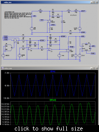
Here it is in 'regulation',


Start Up will give you 'Kittens' but I should imagine there is a way of overcoming that.

Genome
 
Last edited:

Genome, thank you very much for reading my thread and contributing an above and beyond reply. I have been having a rather hard time getting any help from Maxim. Before I started drawing a schematic or calculating the first component value I called Maxim and told them what I was planning to do with this driver. They assured me the driver will work for my needs and as long as I didn't overload the gate driver, I could create any size design I wish.

Before I scrap this design, I would like to get to the bottom of the issues, at least just for my own education. I've sunk a considerable amount of time and money in this and the least I should get is an expensive education! That said, I'd very much like to take a look at your cuk design. Are you offering to work with me through this to completion? The additional items needed on this power supply are an external 0 - 10v analog input to give 0 - 100% output to the LED's, it also needs a very fast on/off time as some applications will require it to work as a strobe light power supply. Reaction needs to be on time 3us off time 2us.

To design my circuit, I followed the equations in the datasheet and also a spreadsheet. However, the datasheet and the spreadsheet used slightly different equations for the loop compensation which gave wildly different answers. As in 29.1r, 0.68uF and 270nF with one set of equations and 690r, 6.8uF and 270nF with another set of equations. Nether values seem to set up the perfect waveforms on the inductor or fets. It makes me wonder if the biggest problem here is the loop compensation. As I cant get a straight answer from Maxim, I'd like to spend a some time to learn how to calculate and correctly design loop compensation. Maybe then this design will work and I can put that knowledge to use with the cuk circuit.

In the meantime, I'm building your schematic in LTSpice and looking forward to playing around with it.

One other thing that crossed my mind was to create a buck/boost using a PIC as the driver. This would create a completely customizable solution.
 

Again I think the data sheet, and the suggested topologies (boost/sepic or otherwise) are tailored to much lower power levels than those which you are trying to achieve. Perhaps the IC can drive the beast it's just that the beast being driven has become unruly.

My guess, based on your component values and operating frequency, is that you have followed a design procedure for a much lower level power circuit on the assumption that it makes a transition from discontinuous operation to continuous operation at about half the maximum output current and attempted to use the same design procedure the note offers and then things went sort of wrong.

Try this,


Code:
* C:\LED\ledboost.asc
LIN N001 VIN 8.2µ
S1 0 N001 DRV 0 MSW
D1 N001 VOUT DID
VIN VIN 0 26V
A1 VDD 0 CLK 0 PWM 0 DRV 0 DFLOP Vhigh=15 Vlow=0 Trise=50n Tfall=50n Td=10n
S2 PWM 0 VTRI VVEA CMP
R8 VDD PWM 1K
VDD VDD 0 15V
V§CLK CLK 0 PULSE(0 15 0 10n 10n 500n 12.5u)
V§TRI VTRI 0 PULSE(5 1 0 12u 500n 0 12.5u)
XU1 N002 0 VVEA opamp Aol=100K GBW=10Meg
C3 N003 N002 4n7
R3 VVEA N003 10K
D2 N002 VVEA ZID
VLED VOUT VIN 26V
B1 ISNS 0 V=I(LIN)
R1 N002 ISNS 100K
R2 N002 N004 100K
V§IDEM N004 0 20
.model D D
.lib C:\Program Files\LTC\LTspiceIV\lib\cmp\standard.dio
.MODEL MSW SW(RON=1m ROFF=1E9 VT=5)
.MODEL CMP SW(RON=10m ROFF=1E9 VT=0)
.MODEL DID D(RON=1m ROFF=1E9)
.MODEL ZID D(RON=10m ROFF=1E9 VREV=6V)
.tran 0 1.1m 1m 10n uic
.LIB OPAMP.SUB
.backanno
.end

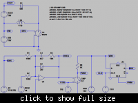
I am guilty of not looking too closely at the Maxim data sheet to see how it thinks it might be working but the upper section is representative of your power stage. VIN is Boosted up over VIN to VLED sitting on top of VIN.

I've set VIN and VLED to be 26V which should give me, ignoring other things, something like a 50% duty cycle. Otherwise it is a bit of a 'Fudge' but does demonstrate some of the issues in your present circuit.

The 'Fudge' is the way I am controlling things. That is the lower half of the circuit. I am measuring and controlling 'inductor' current rather than 'output' current. I'm sure the Maxim circuit does something slightly different but that is not going to affect the resulting waveforms.

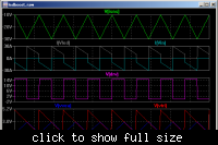
Using your 8.2uH, operating at 80KHz and asking for 10A, total from IDEM set to 10V which will be 5A in and 5A out, gives,


V(ISNS) demonstrates the peak inductor current of 20A.

I(VLED) and I(VIN) demonstrate the peak 20A sawtooths at 50% duty cycle. They average to 5A. Half Peak and half again.

V(DRV) shows the 50% duty cycle.

The bottom curves just demonstrates 'slope matching' in the error amplifier being used to control things.

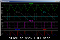
If I set IDEM to 20 for 10A in and 10A out, with 10A out being your maximum figure then the result is,


The inductor current has become continuous (and it will gain the Right Half Plane Zero) but, and I did not spot this until I modelled it, both the input and output currents remain discontinuous and that makes your input and output filtering problems even worse.

If you moved to SEPIC you might improve the situation on the input but the output would still suffer in a similar manner.

A CUK converter will place the stresses elsewhere but, comparatively speaking, that might/will be more manageable. Certainly the input and output currents are not subjected to such extremes in terms of ripple. The switch and the coupling capacitor get to suffer instead....

I realise you have an investment in time, money, sweat and stress over what you have tried so far. I don't believe you will be able to improve the situation without moving to a different topology. Having said that I am just some 'nutter' who has turned up on the internet proposing CUK and I know for myself that they have not behaved for me in the past.

This time, the previously presented CUK model, it 'seems' to have worked.

100%, equates to best I can. Just you make sure you check on what I might propose and how it is meant to work. Hopefully I will be able to give supporting information. Drop me when you get 'worried'.

Genome.
 
Last edited:

Status
Not open for further replies.

Similar threads

Part and Inventory Search

Welcome to EDABoard.com

Sponsor

Back
Top