Continue to Site

Welcome to EDAboard.com

Welcome to our site! EDAboard.com is an international Electronics Discussion Forum focused on EDA software, circuits, schematics, books, theory, papers, asic, pld, 8051, DSP, Network, RF, Analog Design, PCB, Service Manuals... and a whole lot more! To participate you need to register. Registration is free. Click here to register now.

Help with spec'ing FETs for 11A @ 26V led driver

Status
Not open for further replies.

JMG

Member level 3
Member level 3
Joined
Sep 27, 2005
Messages
66
Helped
0
Reputation
0
Reaction score
0
Trophy points
1,286
Activity points
1,908
I have a buck-boost design that currently works ok-ish. At 27 - 40Vin the driver is stable and delivers full load. At 22 - 27Vin the output caps squeal and the output is electrically noisy. The design calls for 22 - 40Vin so this needs to be fixed.

I have spoken with tech support for the driver IC and after looking through my numbers, schematic and layout he thinks its FET related, and if that doesnt fix it my current sense needs to be a little closer to the driver IC.

He thinks the gate charge is too high. I have 2 FETs in this design and one gets hotter than the other yet they are both in parallel and next to each other on the pcb. I am using 2x STB75NF20's and he is recommending I change to 2x IRF6646's.

My understanding of FET's appears to be limited so could someone explain to me how 2x 2.8W FET's are going to work when switching 286W of load?

Thanks.
 

We are suppose to guess what the schematic looks like?
 

Attachments

  • YJ5Driver-Maxim.pdf
    110.5 KB · Views: 170
  • irf6646.pdf
    652 KB · Views: 135

I don't think it's a current sense problem. You sense the same
current all the time (or try). But low line problems may mean
you have either an input-side current problem, or are up against
a duty cycle limit. That the caps' squeal becomes audible, may
mean you have gotten so much duty that you are starting to
skip pulses.

Missing from all this discussion is a single set of switching
waveform 'scope plots, driver output and inductor input
node data are worth more than any amount of speculation.
One normal, one abnormal, the problem would likely show.
 

The schematic is for a boost only design. In the schematic, why is LED - tied to Vin?

What confused me it you say it only works for input voltage above desired output voltage.

That would seem to imply to me the switcher is not working at all. The fact that it works with input voltage above needed LED voltage is because of the dimming MOSFET duty cycling to control LED current.

My first suspect would be switcher coil. Are you sure it is large enough to ensure it is not saturating its core?
 
Last edited:

Ok let me try and answer all those points.

The design is copied pretty much straight from the device datasheet and eval board schematics. Obviously component values are changed. I created a spreadsheet using the datasheet equations and had it ran through by the Maxim engineers. Its ok and all the numbers should be correct for any combination of input and output.
It should be a buck-boost with Vin min = 22V and max = 40V. The driver works from 27 - 40Vin but below 27V it does not. Well, it does if you limit current to 5A.


The inductor is 8.2uH with a 42A saturation current and a 30A avg current. Calculated currents at 22Vin are around 29.9A peak and around 24.5A avg. The coil should not be saturating. Also just fyi, it does not get hot.
Calculated duty cycle at 22Vin should be 55.05% but I have seen 99% at full load. Maxim eng's say this is FET related - too much gate charge and so I should change to the irf FETs with lower gate charge.
Although the datasheet says a min switching frequency of 100kHz, I'm running at 80kHz and this was approved my Maxim. Actually they suggested 70 or 75kHz but I found the problems got worse lower than 80kHz.

The dim Fet is externally controlled. I do not use pwm dimming but it is used as a remote on/off switch. I use the analog dim which works very well. There is a problem with the pwm dim circuit though. If the dim is turned on (pulled high) and input power is applied, the device will max out the bench power supply to its current limit and latches in this state. Power has to be removed and the pwm dim pin brought to ground before power up again and normal function occurs. Maxim have no answer for this.

I've had several other issues too. The numbers call for a 68uF cap on the input and 330uF on the output. I used a single low esr Panasonic aluminum elec 100V on the input and a single Panasonic aluminum elec on the output. Both caps got hot, with the input cap getting very hot. Changed the input side to 1x high esr 330uf 100v elec, the original 68uf, 5x 22uf ceramics and 1x 1uf ceramic. The output is now 1x 330uF high esr elec, 1x 33uF high esr elec, 10x 22uf ceramics, 1x 4.7, 2.2 and 1uf ceramic. This has solved the ripple and electrical noise issues. The input ripple is 1.9V pk - pk, the output is 2.5V pk-pk at 10.5A 25.4V with 40V input.

Also at 40V input it draws 10 - 10.5A. The output is measured as 25.4V at 10.5 - 11A. So 400W is being pulled to run a 286W load in buck mode. Something is obviously wrong.

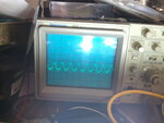
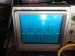
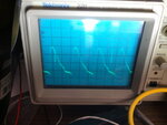
I dont have any plots to show you at the moment other than 3 I took of the output before I fixed the ripple issue. My last driver just died due to me accidentally shorting the Vin pin (40V) to the 7v regulator output pin. It will be Thursday next week before more get here. I planned on re-laying out the pcb to accommodate the new FETs in the mean time.

LINKS:

Device datasheet: **broken link removed** Take a look at the typical circuits at the bottom of page 20 called Buck-Boost headlamp driver.

Evaluation board datasheet: **broken link removed**

Inductor datasheet: **broken link removed**

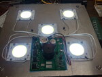
Scope pictures and pdf's of the layout and a pic of the pcb attatched.
 

Attachments

  • YJ5Driver-maxim-bot.pdf
    92.9 KB · Views: 125
  • YJ5Driver-maxim-top.pdf
    126.3 KB · Views: 114
  • YJ5Driver-maxim-topsilk.pdf
    100.3 KB · Views: 157
  • 1Amp.jpg
    1Amp.jpg
    1.6 MB · Views: 137
  • 3Amps.jpg
    3Amps.jpg
    1.5 MB · Views: 127
  • 8.5Amps.jpg
    8.5Amps.jpg
    1.5 MB · Views: 135
  • 2010-10-05 20.03.54.jpg
    2010-10-05 20.03.54.jpg
    1.6 MB · Views: 129
Last edited:

Just had a thought. Shouldnt the output caps be across the LED's and not LED anode to ground?
 

Just had a thought. Shouldnt the output caps be across the LED's and not LED anode to ground?

I am still trying to figure out why schematic has LED- tied to + supply. Your LED- must be hooked to ground or you would not be getting anything.

Also P-ch MOSFET dimmer device is hookup up backwards with drain and source reversed.

It is only a boost circuit. The MAXIM data sheet specifically mentions a SEPIC design for buck-boost but offers no applications schematic for a SEPIC hookup. It only show an application schematic for a boost design.

The NDRV spec for Nch MOSFET driver is +/- 3 amp, 30 ns rise/fall time with 10 nF load. That is enough drive for pretty large MOSFET. PGND, pin 13, needs a heavy trace connection directly to ground pads on R4 or you will be jacking the whole rest of the IC circuit up in the air.

It's not the coil that will necessarily get hot when it saturates, it is the MOSFET's. 99% duty cycle (assuming you are refering to MOSFET's) would guaranty coil saturation.

Have you tried to see if boost circuitry is functioning with a lighter load?
 
Last edited:

I am still trying to figure out why schematic has LED- tied to + supply. Your LED- must be hooked to ground or you would not be getting anything.

The eval circuit shows this same configuration for buck-boost operation. But I agree, I've looked around the net and have seen several examples of buck-boost drivers where the LED cathode is grounded. The other power components have the same configuration as this design. Then again I saw a TI app note for a buck-boost connected exactly the same as this circuit.

Also P-ch MOSFET dimmer device is hookup up backwards with drain and source reversed.

Fixed. Good eye! This could fix a lot of issues such as the latching on problem. Weird how it still worked though. So the drain goes to the LED anodes and the source towards the diode.

It is only a boost circuit. The MAXIM data sheet specifically mentions a SEPIC design for buck-boost but offers no applications schematic for a SEPIC hookup. It only show an application schematic for a boost design.

There are 2 schematics on page 20. I followed the last one labeled as buck-boost headlamp driver. Are you saying this schematic is labelled wrong?

The NDRV spec for Nch MOSFET driver is +/- 3 amp, 30 ns rise/fall time with 10 nF load. That is enough drive for pretty large MOSFET. PGND, pin 13, needs a heavy trace connection directly to ground pads on R4 or you will be jacking the whole rest of the IC circuit up in the air.

I agree with the fet drive. There is an equation in the datasheet which tells you max gate charge. Max drive is 3A so drive I = Qg x fSW so .000000084 x 80000 = 6.72mA per FET.
Pin 13 has 245.9mils of 20mil wide trace then is connected by via to the ground plain at R4. I can increase that trace thickness.

It's not the coil that will necessarily get hot when it saturates, it is the MOSFET's. 99% duty cycle (assuming you are refering to MOSFET's) would guaranty coil saturation.

Have you tried to see if boost circuitry is functioning with a lighter load?

Yes it was the gate duty cycle I was referring to. The circuit works perfectly from 22 - 40Vin with a load up to 5A. The more load above 5A added, the more input voltage is needed until at 27Vin it will supply the full load but squeal. The more input voltage above 27Vin, the quieter it gets.

Something I didnt mention earlier was I put 10uF caps across each LED's terminals and this reduced a lot of audible and electrical noise, and brought the full load operating voltage down to 27V from 35V.
 

Figured out why the led cathodes are connected to vin. This is an input referenced buck -boost design. My schematic is correct.
And further thinking has got me to realize that buck mode works fine but boost mode can't supply the full load.
 

Page 20 is not a buck-boost switcher. It is a boost only. Hooking LED neg. to Vin supply means boost switcher must always raise LED pos. voltage above supply to power the LED. Switcher output is always Vin + LED forward voltage.

Not a good design as there will always be more switcher loss because it always has to boost the LED+ supply above input voltage. Could have stability problems if Vin does not have a low impedance since LED current is injected back into Vin supply line. (output current injected back into input).

The IC has no Vgs bootstrap for N-ch MOSFET driver. It's MOSFET driver is fed from a 7v internal regulator. This is a relatively low voltage for power MOSFET's. You have to find a N-ch MOSFET that has Rds-ON you need at about 6 volts Vgs. Finding a MOSFET with the Rds-ON you need with only 6 volt Vgs is going to be very difficult. The higher the Rds-ON, the hotter the N-ch MOSFET will get.

At input of 40 volts and an LED that requires 26 volt plus some drop for sense resistors and P-ch MOSFET dimmer you are going to exceed the chip's max voltage boost of 65 vdc. The Isense+ input is being subjected to the boost output so its sense amp devices will be where breakdown will occur. Hopefully the overvoltage sense will shut down switcher.

A SEPIC design is an actual buck-boost switcher and LED- would be tied to ground.
 
Last edited:

Ok i see and agree with all your comments. As Maxim have given me a recommended fet to use, would you say that this circuit as is would work correctly if I connected the led cathodes to ground? Would I get my buck boost driver?
 

The MOSFET's they recommended are better then the ones you originally used but not great. Take a look at their specs. The spec for Rds-ON starts to shoot up at below 7 volts Vgs, not giving you much margin for Rds-ON degradation for temp rise.

I don't know of any specific MOSFET's better to recommend. Lower Vgs for good Rds-ON usually comes on MOSFET's with lower Vds breakdown. You can find alot with 50v breakdown but that won't do for your need. You might find something better with 100 v MOSFET's. You should be able to get by with 100v MOSFET's with max of 65 volt boost, just be careful of too much overshoot on trailing edge of conduction. Maybe some small degree of R-C snubbing on drain to ground will help if you see too much overshoot.
 

So really we are back to square one. Going back to what Dick said, he may be on to something as I seem to recall looking at the duty cycle rise considerably with lower input voltages. If I have ran out of headroom, would this mean my inductor needs to have a higher current rating due to saturation? The calculation says I should be at 55.05% at maximum load with 22Vin. Fortunately I do have a higher rated inductor to test but no more drivers until they arrive in a few days.
 

New drivers arrived early. So yeah, confirmed that there is a very high duty cycle when the input voltage is less than the voltage across the LED's. Any pointers on how I fix this?
 

You should run a simulation. You don't need a MAXIM model, just a variable duty cycle driver.

Your duty cycle at 27 vdc supply should be about two thirds charge, one third discharge. The fact that it quits at close to LED forward voltage supply level is only coincident. The boost switcher must produce 26 v above supply. At 27 vdc supply that would be 53 vdc @ 11 amps on switcher output. It only means switcher cannot produce the 11 amps at 53 vdc when supply drops below 27 vdc.

At 85 kHz and 8.2 uH you can't make that in a discontinuous switcher mode. It takes about 20 usecs to charge 8.2 uH coil for the required 66 amps of peak current in discontinuous mode. From specs it is not clear the MAXIM part can run in continous conduction mode which would reduce the peak coil current. You will still see 2/3 charge, 1/3 discharge cycle in continuous conduction mode (when it reaches steady state) at 27 vdc supply & 53 vdc @ 11 amps output.

You need to reduce freq or decrease coil value. For 8.2 uh (with 66 amp peak current) you cannot run higher then about 30 kHz, assuming coil does not saturate.

Sorry, but this circuit is just bad for two main reasons.

At 22v-40v supply input and 11 amps for LED, the switcher must produce 240w to 440 watts more then the LED's need. The extra loss in doing that is just bad design. Yes, you get 11 amps injected back into supply but that does not help the switcher.

With only <7 volts of gate drive from I.C. it makes it tough to get low Rds-ON and thus efficiency, again, just bad design.

You need a real buck-boost switcher. SEPIC or 4 switch design. SEPIC's are more difficult to design and have a lot of external parts.
 
Last edited:

Your numbers are way different to the results calculated using the Maxim datasheet. I believe it runs in continuous mode as the peak current is calculated to be less than 30A. I've attached a spreadsheet the includes the datasheet calculations so all that has to be done is enter Vin min, Vin max, Vled, Iled, switching frequency etc etc. As I mentioned earlier this spreadsheet was looked over by Maxim, a mistake fixed and sent back to me. See what you think.

Ignore the left column for boost mode only, there is a couple of errors to fix in it.
 

Attachments

  • MAX16833B COMPONENT VALUE CALCULATOR YJ5 DRIVER.zip
    3.6 KB · Views: 95

Your numbers are way different to the results calculated using the Maxim datasheet. I believe it runs in continuous mode as the peak current is calculated to be less than 30A. I've attached a spreadsheet the includes the datasheet calculations so all that has to be done is enter Vin min, Vin max, Vled, Iled, switching frequency etc etc. As I mentioned earlier this spreadsheet was looked over by Maxim, a mistake fixed and sent back to me. See what you think.

Ignore the left column for boost mode only, there is a couple of errors to fix in it.

I may have put too much loss in circuit. What diode are you using and what is series resistance of coil?
 
Last edited:

Diode is SBG3060CT-T-F
Digi-Key - SBG3060CT-T-FDICT-ND (Manufacturer - SBG3060CT-T-F)

Inductor resistance is 0.004 ohms.
**broken link removed**

You realize the diode has a 60v breakdown spec. That will be a supply high end problem.

You only show one diode in layout, while two on schematic. Either way the diodes are going to cook just surface mounted without heat sink. At 22 vdc supply, the power dissipation on two diodes in parallel is 6.6 watts. For a single diode it is 11.5 watts.

Avg. coil current is 26.3 amps, peak 35.2 amps, min 17.5 amps.

Duty cycle 57%. MOSFET dissipation (for pair) is 3.3 watts.

With the diode and MOSFET's mounted together at bottom right corner of PCB, with about 14 watts of dissipation needed, you will probably melt the solder on components in that corner of board.
 
Last edited:

Status
Not open for further replies.

Similar threads

Part and Inventory Search

Welcome to EDABoard.com

Sponsor

Back
Top