danaoxm
Newbie

Help Needed with 16-Bit Bit Zero Detector Circuit Design
Hi everyone,
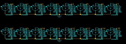
I’m working on designing a bit zero detector circuit that takes a 16-bit input and outputs two signals: one if the number of zeros is greater than 7, and another if it’s greater than 11. This circuit will be used to control charge pumps in non-volatile memory programming. I’m using Mentor Graphics tools (Pyxis, Eldo, Calibre) for this project.
Here’s my setup so far:
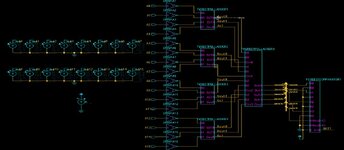
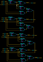
• Each input bit (A0 to A15) is connected to an inverter.
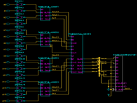
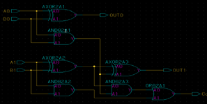
• The inverted bits are grouped into pairs and connected to 2-bit half adders.
• The outputs from the 2-bit adders (S0, S1, and Cout) are then connected to a 4-bit full adder to accumulate the zero count.
• Finally, the output of the 4-bit adder is connected to a 5-bit comparator to check if the zero count exceeds the thresholds of 7 and 11.
Issue: The generated waveform doesn’t match the expected output, and I’m not sure why. I’ve checked the connections and logic, but the problem persists. I suspect there may be an issue with carry propagation, timing, or the comparator configuration.
Any advice or suggestions on where I might be going wrong?
Thanks in advance for any help!
