Continue to Site

Welcome to EDAboard.com

Welcome to our site! EDAboard.com is an international Electronics Discussion Forum focused on EDA software, circuits, schematics, books, theory, papers, asic, pld, 8051, DSP, Network, RF, Analog Design, PCB, Service Manuals... and a whole lot more! To participate you need to register. Registration is free. Click here to register now.

Help me understand a paragraph from a book (001)

Status
Not open for further replies.
as to your final question, yes adding a series Re is the best way to match transmission line and for higher currents, one can neglect Zout as ~0 and simply use a series Re=49.9 Ω 1% for RF, unless you have other requirements.

Now go look at some specs for transistors and use worst case β Max/min and consider my previous advice.

EDIT referring to the Common Emitter Q point question elsewhere you posted today. :(
 

Did you mean to replace RE= 1K by RE=49.9 Ω 1%? If you mean that it means to modify the bias.

Actually I meant and said series Resistor so 50 instead of 43. But that reminds me of another problem.
Now that you add 50 R Series and 50R load the Emitter sees a capacitively coupled 100R so voltage output limited by the DC bias current..ie 5ma*100 Ohms=500mVpp ( with 50 series & 50 load) reducing 1K to increase bias current allows a bigger output swing AC connected load connected to Re on the emitter.

5.jpg
 
Last edited:

Actually I meant and said series Resistor so 50 instead of 43. But that reminds me of another problem.
Now that you add 50 R Series and 50R load the Emitter sees a capacitively coupled 100R so voltage output limited by the DC bias current..ie 5ma*100 Ohms=500mVpp ( with 50 series & 50 load) reducing 1K to increase bias current allows a bigger output swing AC connected load connected to Re on the emitter.

May be I miss a point in the discussion. Provided a simple hand calculation as in post #2 shows an amplifier output impedance of about 7 ohm, why would you ignore it and choose 49.9 Ohm +/- 1 %?.

The more interesting question is about circuit large signal behaviour. Please notice that all calculations in this thread are referring to small signal parameters only. Designing the circuit for a specific output signal level is a different topic. You are leaving the simple world of small signal approximations and transiting to non-linear circuit descriptions. You have to face the fact that any real transistor circuit adds distortions to the input signal, choosing a bias level presumes an amount of acceptable non-linearity and signal distortion.
 

Hello Samy555, I am sorry, but I feel the necessity to give some additional explanations (and comments to post#19).

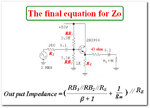
Output impedance = (3.3k//3.3k//200)/beta + (re//RE)
Is that true?
No.... test it for zero values of RE.
If you consider the transistor Rπ as part of the source impedance where (β+1)*Rbe= Rπ
Then you get my generalized solution Zout = all source impedances/current gain
Setting RE=0 is no counter argument because for RE=0 you have no emitter follower anymore. This assumption makes no sense.
What is the physical representation of (β+1)*Rbe= Rπ ? What do you mean?

Changing labels for RE = Re and re=Rbe and beta=β
I see it as ...
Zo=(3.3k//3.3k//200)/(β+1) // Re + Rbe
= 178Ω/(β+1) // Re + Rbe
= 1.8Ω // Re + Rbe
= 1.8Ω + 25Ω /Ie
= 1.8 + 5 = 6.8Ω ( they got 7.8)
Note for Rbe above from Ebers-Moll equation
I = I s [e^(qV/ kT) -1] you can derive Rbe for T=25'C where Rbe=25 [Ω]/Ie [mA] of emitter current.
thus if Vc=6V across 1.2k Ic=5mA then Rbe=5Ω

This part is causing some confusion (at least on my side). Why changing labels?
In particular, re=Rbe ??? In all books I know it is the the base-emitter resistance which is named rbe (identical to hie=rπ, see the equivalent small signal diagram in post#3).
This value can be derived as rbe=26mV*beta/4.4mA=591 Ohms. (What is the PHYSICAL meaning of the quantity Rbe=5 Ohm, as shown in post#19 ?).
____________________
Samy555 - I am afraid, you are somewhat confused about all the different formulas.
However, it is very easy to proof which formula is correct if you understand the physical background.

Here is my explanation in words:
* It is a known fact (which can be found in each textbook) that the input resistance at the emitter node in common base configuration is the base-emitter resistance divided by the factor Ie/Ib=beta+1.
Because this, obviously, is identical to the output resistance (let´s call it r2) in common collector configuration (firstly, without consideration of the base circuitry) we have r2=rbe/(beta+1).
Neglecting the "1" this gives the commonly used resistance at the emitter node r2=1/gm. (It is easy to show WHY rbe/beta=hie/hfe=1/gm).
* In contrast to common base, here we have a base circuitry which must be added [divided by (beta+1), because of Ie/Ib=(beta+1)]: Thus, we add Rsource=(RB1||RB2||RS)/(beta+1)
* Because the series connection (r2+Rsource) is in parallel to the ohmic emitter resistor RE we, finally, arrive at the resulting output resistance
r,out=(Rsource+r2)||RE.

Introducing the given values (post 1) with beta=100, Ic=4,4mA we arrive at
Rsource=178.4/101=1.77 Ohms
r2=1/gm=Vt/4.4mA=26mV/4.4mA=5.91 ohms
r,out=(1.77+5.91)||1000=7.68||1000=7.62 ohms.

As we can see, the resistor RE - as expected - plays a minor role because the resistance at the emitter node always is in the lower Ohm-range.
I hope this can clarify something - because the formulas can be explained and verified.
 
Last edited:
  • Like
Reactions: samy555

    samy555

    Points: 2
    Helpful Answer Positive Rating
The more interesting question is about circuit large signal behaviour. Please notice that all calculations in this thread are referring to small signal parameters only. Designing the circuit for a specific output signal level is a different topic. You are leaving the simple world of small signal approximations and transiting to non-linear circuit descriptions. You have to face the fact that any real transistor circuit adds distortions to the input signal, choosing a bias level presumes an amount of acceptable non-linearity and signal distortion.
The book referred to in post #1 and in the same page (2-11) talk about that point and I intend to talk with you about it, but I waited for the end of the debate on the first question.

- - - Updated - - -

Setting RE=0 is no counter argument because for RE=0 you have no emitter follower anymore. This assumption makes no sense.
Yes yes yes.
You're right
Exactly, the lack of RE eliminates the work of the circuit as an emitter follower
____________________
Samy555 - I am afraid, you are somewhat confused about all the different formulas.
However, it is very easy to proof which formula is correct if you understand the physical background.
Thank you for the noble feelings.
Here is my explanation in words:
* It is a known fact (which can be found in each textbook) that the input resistance at the emitter node in common base configuration is the base-emitter resistance divided by the factor Ie/Ib=beta+1.
Because this, obviously, is identical to the output resistance (let´s call it r2) in common collector configuration (firstly, without consideration of the base circuitry) we have r2=rbe/(beta+1).
Neglecting the "1" this gives the commonly used resistance at the emitter node r2=1/gm. (It is easy to show WHY rbe/beta=hie/hfe=1/gm).
* In contrast to common base, here we have a base circuitry which must be added [divided by (beta+1), because of Ie/Ib=(beta+1)]: Thus, we add Rsource=(RB1||RB2||RS)/(beta+1)
* Because the series connection (r2+Rsource) is in parallel to the ohmic emitter resistor RE we, finally, arrive at the resulting output resistance
r,out=(Rsource+r2)||RE.

Introducing the given values (post 1) with beta=100, Ic=4,4mA we arrive at
Rsource=178.4/101=1.77 Ohms
r2=1/gm=Vt/4.4mA=26mV/4.4mA=5.91 ohms
r,out=(1.77+5.91)||1000=7.68||1000=7.62 ohms.

As we can see, the resistor RE - as expected - plays a minor role because the resistance at the emitter node always is in the lower Ohm-range.
I hope this can clarify something - because the formulas can be explained and verified.
Yes, the explanation was very clear and convincing.
And I will consider it as the right end of our useful dialogue
Thank you

4.jpg
 
Last edited:

Samy555 - thank you.
There is another simple method to derive the final formula directly from the small-signal equivalent diagram as shown in post#3. Perhaps you are interested.

1.) Setting the input signal Vs=0 and applying a test voltage Vo at the output it can be seen that there is one current through the node E which according to Ohm`s law is Io,1=Vo/(rπ+Rsource)
With "our" symbols rπ=rbe=hie and Rsource as before we have Io,1=Vo/(rbe+Rsource)
2.) However, there is another current through the output node E caused by the current source which is Io,2=beta*Io,1 (because Io,1 is identical to the current through the base node B)
3.) Thus, we have Io=Io,1+Io,2=(1+beta)*Vo/(rbe+Rsource).
4.) Hence the output resistance is
rout,1=Vo/Io=(rbe+Rsource)/(1+beta)=Rsource/(1+beta) + rbe/(1+beta)
5.) Neglecting the "1" in the 2nd part and setting rbe/beta=hie/hfe=1/gm (this is a known relation, simple to prove)
we finally arrive at
rout,1=Rsource/(1+beta) + 1/gm
6.) Taking RE into consideration, we have
r,out=rout,1||RE.

( q.e.d.)
 

Hello all
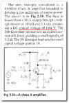
Near the end of page 2-11, I read:
6.jpg
The DC emitter voltage (VE) ≠ 1.64 V as the author said!
Lets calculate it:
VB = VCC * [3.3K/(3.3K+10K)] = 2.48 V
VE = VB - VBE ,,,, The author always assumed that the value of VBE = 0.7 V, so,
VE = 2.48 - 0.7 = 1.78 V
The question is:Who among us wrong??
Thank you very much
 

Vbe tends to be higher for RF transistors in GHz with very low Ic max ratings. That would be overkill here for 160MHz GBW at 10mA and then tends to be lower with high current use of a high rating.

I would say you were closest at 1.64V rather than 0.84V drop at 8.2mA
Then your current would be 1.78/200=8.9mA

not much different as the AC current controls the gain with the bypass cap.
 

Here's your error
Lets calculate it:
VB = VCC * [3.3K/(3.3K+10K)] = 2.48 V

Please review the previous discussion. The voltage divider is additionally loaded by the base current, so VB must be lower than 2.48 V. As far as I see, transistor beta isn't specified for the example circuit, so you are unable to calculate the exact voltage levels.
 
  • Like
Reactions: LvW

    LvW

    Points: 2
    Helpful Answer Positive Rating
Vbe tends to be higher for RF transistors in GHz with very low Ic max ratings. That would be overkill here for 160MHz GBW at 10mA and then tends to be lower with high current use of a high rating.
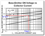
2N3904 datasheet says:VBE (on) ≈ 0.72 V @ IC= 8mA
7.jpg
There is no data about the relation between Vbe and frequency. Note that the amp operating frequency is not so high (GHz), it is only 10MHz
I would say you were closest at 1.64V rather than 0.84V drop at 8.2mA
Then your current would be 1.78/200=8.9mA
not much different as the AC current controls the gain with the bypass cap.
I know they are close, but the author meant that value of specific, and I hope to know why.
Thank you SunnySkyguy very much

Here's your error


Please review the previous discussion.
Does not need to review the previous discussion, Everyone calculated VB in that way.
The voltage divider is additionally loaded by the base current, so VB must be lower than 2.48 V.
I know that if the divider current in the 10K = 10 * IB, then the current in the 3.3K resistor = 9 * IB, but this, but that does not make this big difference!
As far as I see, transistor beta isn't specified for the example circuit, so you are unable to calculate the exact voltage levels.
Author always supposed that β = 100 at DC
Thank you FvM very much
 

Hello
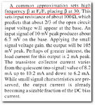
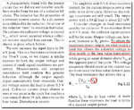
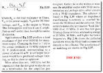
I continued reading, the author says at the beginning of page 2-12
8.jpg
While in the 2N3904 datasheets:
9.jpg
Datasheet says that β @ 10MHz ≈ 35. You might say they are approximately eaqual,,, OK

but at freq = 100MHz, β in datasheets ≈ 16, while ccording to the expression (β=Ft/f), β=300/100 = 3, they are not approximately eaqual.

My question is: Any way of them must be chosen When I want to calculate β?
thank you very much
 

Note that the current gain in the datasheet is expressed in decibels. So at 100MHz, current gain = 16dB = about 6. That makes sense, since according to that datasheet Ft = about 600MHz.

Similarly, at 10MHz, 35dB means a gain of about 56, pretty close to 600MHz/10MHz.
 
  • Like
Reactions: samy555

    samy555

    Points: 2
    Helpful Answer Positive Rating
Note that the current gain in the datasheet is expressed in decibels. So at 100MHz, current gain = 16dB = about 6. That makes sense, since according to that datasheet Ft = about 600MHz.

Similarly, at 10MHz, 35dB means a gain of about 56, pretty close to 600MHz/10MHz.

Thank you very much
You really helped me. You pointed to a point of great significance
Thank you again
I am very happy because I received a wonderful answer

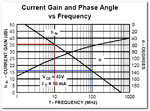
Remained a small problem which we all know that Ft of the 2N3904 is 300MHz,, look:
1.jpg
How it is in the curve above = 600MHz??
thanks
 

The printed spec's in the datasheet say the minimum fT is 300MHz. The graph curves are for "typical" devices that are twice as good as the minimum spec'd ones.
 
  • Like
Reactions: samy555

    samy555

    Points: 2
    Helpful Answer Positive Rating
The printed spec's in the datasheet say the minimum fT is 300MHz. The graph curves are for "typical" devices that are twice as good as the minimum spec'd ones.
**broken link removed**
This day is a happy day. I've got great answers from more than wonderful friends.
Thanks alot
 

Hi
After the last paragraph in the post #31, I read:
3.jpg
4.jpg
5.jpg
6.jpg
7.jpg

My question: Is saturation occur really when VC = VB?
Thank you
 

I think they meant "...that allows the collector voltage to drop nearly to the emitter voltage (saturation)".
Collector voltage can normally go below base voltage before saturation happens.
 
  • Like
Reactions: samy555

    samy555

    Points: 2
    Helpful Answer Positive Rating
Status
Not open for further replies.

Part and Inventory Search

Welcome to EDABoard.com

Sponsor

Back
Top