Continue to Site

Welcome to EDAboard.com

Welcome to our site! EDAboard.com is an international Electronics Discussion Forum focused on EDA software, circuits, schematics, books, theory, papers, asic, pld, 8051, DSP, Network, RF, Analog Design, PCB, Service Manuals... and a whole lot more! To participate you need to register. Registration is free. Click here to register now.

Friends, help to find out the bug of this charger

Status
Not open for further replies.
It's nice to see someone else with schematics on paper all over the desk - it stops me feeling I'm the most untidy person in the World :)

I think the point you are making is that the current changes path depending on it being in current limit or under microprocessor control. That isn't exactly true but you are on the right lines. The thing to remember is the 338 is an adjustable regulator and the output voltage it produces is set by the voltage on the 'Adj' pin.

Now imagine Q1, Q2 and Q3 do not exist, the only components to set the output voltage are the resistors. The 0.1 Ohm resistor is so small it plays almost no part in setting the voltage so ignore it, the other two resistors are a potential divider, they DO set the output voltage. The purpose of the transistors is to lower the voltage on the 'Adj' pin so the output voltage also decreases, so if all transistors are NOT conducting, only the resistors set the output. For this reason, the resistors are chosen to produce a voltage just a little higher than you actually need.

If Q1 or Q2 conduct, their collector voltages will drop to almost zero and the variable resistors will be in parallel with the 2.4K resistor, reducing it's effective value and dropping the 'Adj' voltage and hence the output voltage. You have control of Q1 and Q2 as they are switched on or off by the microprocessor.

Q3 does exactly the same as Q1 and Q2, it drops the 'Adj' pin voltage if it conducts. The difference is that something else switches it on. That something is the voltage dropped across the 0.1 Ohm resistor. Remember that the transistor will not start to conduct until the voltage between its base and emitter pins reaches about 0.6V and that those pins are connected across the 0.1 Ohm resistor. This means that at 6A, the voltage across the resistor will be 0.6V and the transistor will conduct and pull the output voltage down. It reaches an equilibrium when the reduced voltage, and therefore reduced output current, starts to turn the transistor off again.

To reduce the current at which it starts to limit, Q3 has to conduct sooner so to make it limit at say 3A, the 0.1 Ohm resistor has to be made larger as Pauloynski
explains.

Brian.
 

Hey Brian,
So i'm finalyzing the ckt with the last drawing (Scenerio 1) and just replacing the 0.1Ω with 0.2Ω right??

and then for 3A current, the voltage drop will be .6V right?? And ofcourse still I need an amp to amplify it before feeding it to uC. so for amp purpose, the amp should be not x10 since .6x10 = 6 >>higher than ref. it should be somewhere like x5 or so.... (if i do so...) is it okey then???

[guys, if the whole charger matter finally works well, i have more things to do...]
 

Correct.

The amp would need a gain of 8.33 to give 5V out for 0.6V in, but use a slightly lower gain as the 0.6V is only approximate, it depends on the exact characteristics of Q3 and the resistor value tolerance. If you use a lower gain (about 7 would be my choice) it will ensure you don't hit the top ADC limit if the current is a little higher than expected.

If you use a gain of 7, it will full-scale at 0.715V across 0.2 Ohms which corresponds with output current of 3.57 Amps.

Brian.
 

hey guys,
thanks a lot for all you have done for me... i'll start working on it and will let you know...
 

Dear Sirs,
As i already have started to work on the hardware, can you tell me one thing??? I'm getting confused each and every time...

I wanna use ATMega32. (It's Big enough and actually mega 8 ok... but...)

I want to use the ISP for programming. So The RESET pin will be used for that job. But at the same time, I want a hardware reset using that RESET pin. So What should I do?? Pull-up of 47k and then switch to GND or bla bla bla... can you again give me a tiny schematic (hand drawn is okey as previous) that will do both normal execution, RESET on normal execution and ISP???

Mishu~
 

All you have to do is ensure the programming voltage does not get back to the supply rails. I do not use Atmel processors but PIC devices have the same problem. Your simplest solution is to use a diode somewhere between the supply and reset pin to block the higher voltage. Usually, a single diode voltage drop will still satisfy the devices reset voltage limits.

What are you using at the moment to reset the ATmega32 ?

Brian.
 

hey,
Right now I'm putting it unconnected and keeping a pin/jumper for iSP. but in many schematics, sites, I have seen that it is some kind of...
Code:
                                         |-----------------ISP
                                         |
Vcc<----[10k-47kpull-up]----|------[mega Reset PIN]
                                         |
                                        \
                                         |-----[GND]

but i'm not sure... because at high voltage in RESET pin, atmel goes in to programming mode. the pullup here is just limiting the current and nothing else... the switch takes it low. but i'm not actually sure...

Currently I just down the vcc and then powe it up again....

Added after 5 hours 33 minutes:

Dear Brian,
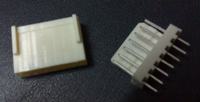
Can you tell me what these connectors are called??? I have to add it in my CAD and i'm planning to use connectors for main ckt and uC part to reduce complexity in building the ckt. I use target 3001 for CAD with LPKF CNC for PCB.

Mishu~
 

The resistor is to isolate the programming voltage from the supply rail. The idea is that the reset pin draws almost no current in normal operation so even 47K can pull the pin right up to the supply voltage. When programming the ATmega you put a higher voltage on the reset pin, supplied from your programming device, but although some current will leak through the resistor, the power line will not rise enough to do any damage elsewhere.

The only thing you need to be careful of is connecting a capacitor from the reset pin to ground. Normally you would add a capacitor so the reset pin rises slower than the supply when you turn the power on. While the processor is running but the reset pin voltage is still climbing, the ATmega will stay in reset mode. This is usually a good idea because it allows the clocks and internal signals time to stabilize before your software starts up. The downside is that the capacitor is also across your programming voltage. I'm not sure if the ATmega just has the voltage placed on the pin or if it carries programming data as well but be aware that the capacitor can have an effect.

The pins have several names but the one I hear most often is "Moles pins" because Molex is a company that makes them. I think the real name is probably 2.54mm PCB headers and shells. They are made in many lengths, straight, right angled and surface mount varieties.

The full information in them is at this web site:
www.molex.com click on 'connectors' then 'wire to board'.

Note that you need a special crimping tool to attach wires to the socket (the plastic shell), I have seen MANY disasters caused by people using pliers or soldering the wires to the terminals.

Brian.
 

betwixt said:
Note that you need a special crimping tool to attach wires to the socket (the plastic shell), I have seen MANY disasters caused by people using pliers or soldering the wires to the terminals.

Please ,can you clarify why soldering is a bad practise? From my practice I can conclude that exactly soldering is the most reliable method. We used to crimp the terminals in the past /automated machine crimping/, but now we solder them. Why? We had quite a lot failed connectors due to oxidized copper core /in view of the fact that connectors aren't sealed/ , resulting in higher contact resistance at the crimped junction -> heat -> accelerated oxidizing -> failure. And this is at normal environmental operating conditions, current lower a few times than specified for the connector,after a period of 2-3 years. Since we started using soldering ,problem disappeared. Although it's a tedious,expensive and time consuming task, for thousands of connectors, done by hand, we do not consider going back to crimping.

Best Regards, Teodor
 

I have had exactly the opposite experience. Soldering gives higher resistance joints than crimping and the heat reduces the springiness of the contact. It also makes a weak spot where the solder wicks up between the wire strands, this is important if the wires will be flexed.

Even if the contacts are soldered, you still have to fold the crimp 'wings' down or it won't fit in the shell.

If you had failures due to oxidization, it would imply your crimps were not folded properly. When fully folded on to the wire it should form a metal to metal compression point which should not let contaminants in to cause problems. I have had experience with tens of thousands of these connectors over many years and I have never seen a single failure of a *properly* fitted crimp. I have seen many failures of wrongly fitted ones, including one that were soldered.

Brian.
 

Dear Brian,
Currently I'm just giving a spot of solder and the cripm with a plier.. works fine... but i have to careful...


well, can you now tell me if the ckt is okey?? then i'll go for making it... specially the part of R1, R8 and Q4?? Still i'm a bit confused....

Mishu~
 

oppssss... accidentally I have missed the 1uF cap between the D2, R1. Dont't worry, it's there...
 

I don't think you really need the three diodes in series with the output but they will do no harm. Consider changing them to Shottky types which will drop less voltage and run cooler. Otherwise it looks OK, even if drawn a little 'unconventionally'.

I can see you might have one problem though. The variable resistors might have to be increased in value or better still, have fixed resistors wired in series with them.
The reason: go back to the formula for calculating the 338 output voltage and calculate it with the resistor set to maximum value. The bottom resistor in the divider will be the 2.4K and 5K in parallel making about 1.6K which will give an output voltage of 10.3V. This is the maximum, you can reduce it DOWN to about 2V but not make it any higher.

If Q1 is the 'power down' control, you can short out the resistor in its collector to get even lower voltage out but check the situation where the charger is switched off completely but a fully charged battery is connected. There shouldn't be a path to feed current backwards where it can reach Q1 but double check.

The diodes in series with Q1, Q2 and Q3 play no purpose whatsoever, you can short them out to make the circuit simpler.

Brian.
 

Brian,

The Diodes for all Qs are because to drop the voltage of AVR's uotput pin. I've seen my AVR gives a voltage of > .7 at LOW. So I need atleast one diode... I will again check because I may need 2.

The diodes (BIG 3s) are for reverse polarity protection. I think they sould work in that case...

I've used all those VRs for many days and they can do well (just I need multi-turn trim pots).

I can see you might have one problem though. The variable resistors might have to be increased in value or better still, have fixed resistors wired in series with them.
The reason: go back to the formula for calculating the 338 output voltage and calculate it with the resistor set to maximum value. The bottom resistor in the divider will be the 2.4K and 5K in parallel making about 1.6K which will give an output voltage of 10.3V. This is the maximum, you can reduce it DOWN to about 2V but not make it any higher.
This part always remained a confusing part for me....

Added after 5 minutes:

about Q1's power-down ctrl, yup... there is a chance of a short path... it is through the GND->Q1_Emmitter->Q1_Collector>resistors>338_output_rail>Batt Positive.
Right?? But it will work to blow the Q1 if the batt is connected reverse. But if the battery is connected in proper polarity, then the EMF from + will not go to the path +>resistor>Q1_Collector>Q1_Emmitter>GND due to the BIG 3 diodes.

(These are my guess only...)
 

If your ATmega32 is producing 0.7V while driving a transistor like this, you have a faulty IC. The data sheet for the ATmega32 says 0.7V maximum WHILE SINKING 20mA but in your circuit it isn't sinking anything. It should go to zero or very close to zero. If you use the diodes, it would be a good idea to add a resistor of about 100K from each base to ground to ensure it stays non-conductive when not being driven.

I think you are looking at the voltage setting circuit as being more complicated than it really is. Just imagine the control transistors are perfect switches, if the base is at 0V (ATmega driving low) the switch is open, if the base has voltage on it (ATmega driving high) the switch is closed. All you are doing by switching the transistor on is adding the variable resistor in parallel with the 2.4K one to lower it's value.

The point I was making about the big diodes is that they are silicon types and will drop about 0.6V. If you are drawing 3A, the power dissipated in them is (W=VxI) 3 x 0.6 = 1.8W so they will get hot. If you use Shottky diodes, the forward voltage drop will be lower, typically 0.4V so the power loss would be reduced to 1.2W.

Brian.
 

Dear sir
here is the schematic. And now if it is okey, then i'll go for making it...

Mishu~
 

oppps.... sorry i did not saw your last post... well, about the switching matters, i think now it's time for practical... if something blows out, well, that will be the lesson for me to learn...

Next about the BIg diods, they have a Drop of .5V (I found) and can deliver current upto 3A (each... so 3x3A 9A total) in normal condition... So let's first try... otherwise dafinitely there is alternative...

so for ATMEGA, only a little change... about the diodes at base... is it like...

Code:
 [From uC]------|>---[10k]---|---[Q_base]
                             |
                             |---[100k]---[GND]

or just a series resistor as [uC]---|>---[100k]---[Q_Base]

???
 

guys,
pcb is ready... started to work on it... will let you know soon...

Mishu~
 

Sorry Mishu, I've been busy elsewhere for the last few days.

If you drive the transistors directly (no diodes) just use a resistor of 10K between the ATmega and the base pin.

If you add the diodes, still use 10K in series with the diodes, but also add 100K from the base pins to ground.

Personally, I can't see any point in using the diodes and you save six components by leaving them out. Just use the 10K in series, it will work fine.

Brian.
 

it's just bull shit!!!!!!

i just finished the assembly and then the R1 of the power ckt just blown up. Also the controller ckt is i dont know why kinda manfunctioning... logic is ok... but ADC is not reading any thing... i even did manual entry... it's just became a bull shit!!!

i'm giving you guys everything i have... so if somebody can fix it...
 

Status
Not open for further replies.

Part and Inventory Search

Welcome to EDABoard.com

Sponsor

Back
Top