Continue to Site

Welcome to EDAboard.com

Welcome to our site! EDAboard.com is an international Electronics Discussion Forum focused on EDA software, circuits, schematics, books, theory, papers, asic, pld, 8051, DSP, Network, RF, Analog Design, PCB, Service Manuals... and a whole lot more! To participate you need to register. Registration is free. Click here to register now.

[SOLVED] flip flops design using latchs

Status
Not open for further replies.
Hi TonyM,

Your description looks mature, and I agree with that.

If you are interested to go in further details then I would recommend reading following book:
CMOS: Circuit Design, Layout, and Simulation, Third Edition by Jacob Baker.

Thanks,
Fpgadsgnr

I'm not sure what you mean by 'mature'...? I can only speak from experience in designing ASICs. I'm glad the posts are calmer, though.
 
Last edited:
I'm afraid Prashanth.vinnakota sounds a bit confused on his understanding of the circuitry. But let's keep this a friendly and helpful forum.

It's true though that people often use 'latch' as a verb for what one does with a flip-flop, probably as there is no obvious verb like flip-flopped'. And 'latch' often gets swapped as a noun for flip-flop. These things often seem to happen in a world containing full of people.

However, the original question was : how can we design a flip flop using latch ?

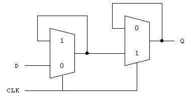
D-type flip-flops (DFFs) in ASICs are usually implemented at low level by two 2-to-1 muxes in series. Each mux acts as a transparent latch by having its output fed back to one of its inputs.

Each mux input select is driven from the CLK signal but uses a different CLK polarity. The first mux latches when CLK=1, the second latches when CLK=0.

74_1341418319.jpg


This is the case in ASICs and the case in Actel PROASICPlus FPGAs, as shown in their data sheet's tile schematic. Though I cannot be certain, I'd say it's highly likely that's the basis of FPGA flip-flops, with extra circuitry to configure the flip-flop to D-type, SR, transparent etc.

Back to the ASIC case...

If it's a rising-edge clocked DFF then:

* When CLK=0, D flows through mux1 to the mux2 input

* When CLK rises, mux1 holds D and mux2 now flows D through to Q

* When CLK falls, mux2 maintains Q while mux1 flows through the next D

...and so on. This makes the CLK edge detection easy and reliable.

Hope this helps answer the original query...

I know this schematic of edge triggered flipflop. But individually each of the MUX acts a transparent latch which contains the clock signal as its select signal. This is a latch and contains clock as its input. So are my earlier statements wrong?

- - - Updated - - -

All i wanted to say is latch is level sensitive i.e each of the mux individually are level sensitive and can be called as latch.

But combinedly they serve as Edge Triggered Flip Flop noting the rising edge of the clock.

This explains and answers the question posted by pulkit.
 

The circuit suggested by TonyM clearly answers the question posted by Pulkit "How to design a flipflop using latches?"

I just want to justify my 1 line statement here which seems contradicting to FPGAdsgnr.

https://obrazki.elektroda.pl/74_1341418319.jpg

-> Each MUX is individually "Level sensitive" as their outputs are in latched state or memory state depending on clock. Hence i give the name latch to both MUXes.

-> Both the MUXes combinedly function as a flipflop because the 'D' input is assigned to 'Q' only when clock changes from '0' to '1'. Its is essentially a Positive Edge triggered Flipflop.
 

Status
Not open for further replies.

Part and Inventory Search

Welcome to EDABoard.com

Sponsor

Back
Top