Continue to Site

Welcome to EDAboard.com

Welcome to our site! EDAboard.com is an international Electronics Discussion Forum focused on EDA software, circuits, schematics, books, theory, papers, asic, pld, 8051, DSP, Network, RF, Analog Design, PCB, Service Manuals... and a whole lot more! To participate you need to register. Registration is free. Click here to register now.

Explanation of AC analysis of oscillator

miki1221

Newbie level 5
Newbie level 5
Joined
Aug 31, 2024
Messages
9
Helped
0
Reputation
0
Reaction score
0
Trophy points
1
Activity points
69
Can someone explain how we do a AC analysis of harmonic oscillator on following example.
I've done the the 16 Mhz oscillator, and simulated it, but I'm trying to understand how it is really working.
zad.png


The equivalent circuit is over here(hope so)
457349066_10233406753181310_6158822657399137013_n.jpg


So my question is, when I start to analyse by hand on paper, I find problem almost on every step, actually I'm not sure if I'm doing it right, so can someone help me go trough it.
I'm very interested in undarstanding of these and simmilar oscillators so, for you maybe this is quite simple, but I'm new in this so everything seems very complicated for me.
I'll be very appreciate if someone finds time to check and answer my question.
Here are results of DC analysis:
1. Ključni elementi kruga:

  • Ucc: 5 V
  • Transistor (Q1): S3018 (NPN)
    • R2=100 kΩ
    • R3=100 kΩ
    • R4=1 kΩ
    • R5=1 kΩ
    • R6=100Ω
    • C16=4.7 nF
    • C15=33pF
    • C15=33pF
  • Kristal:
    • XTAL1=16 MHz
2. (S3018):

  • HFE (β): 200


Ub=2,5V
Rb=50kΩ
UE=1,8V
IE=1,8mA=IC
UC=3,2V
UCE=1,4V

 
Solution
Hello all

After several iterations (building transistor AC model, merging transistor amplifier i/o impedances with impedances of other circuit components, etc) I ended up with below oscillator AC model.
I recognise that it is Pierce crystal oscillator.
For analysis of crystal operation I used this technical note.

Analysis_Pic3a.png


Most challenging for me is to prove phase shift in feedback loop.
Desired phase shift at second (B2) voltage divider is -105deg,
but when I calculate crystal impedance @16MHz and put it into voltage divider equation,
phase shift I got was about -120deg

I used math solver to check possible values of the crystal impedance (and B2 voltage divider gain and phase shift) between the crystal's serial and...
Hello All

It looks like we are reinventing a wheel!
Below is picture from this Microchip technical note
Phase shifts at each stage are similar to my calculations: 75deg and 105deg.
TechNote.png


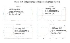
Also I made Bode plots for second voltage divider (B2 stage), and found that it is not so sensitive to change in Cp
I used 0.1pF (0pF plot is not readable and invokes divide by zero in my calculations), 1pF, 3pF and 7pF.
And operation frequency change is several hundreds of Hz.
100fF.jpg
 

Attachments

  • 100fF.jpg
    100fF.jpg
    1.2 MB · Views: 35
Your simulation setup looks basically wrong. Why are you trying .tran analysis? It can be done, but due to high crystal Q, simulation time will be long and you need special measures to achieve oscillation start. uV signal level indicates that you don't get actual oscillations.

Your original question how to perform .ac analysis has been answered.
I didn't understand what you wanted to say, can you explain? now I'm even more confused, what kind of analysis should I try?
 
Hello All

It looks like we are reinventing a wheel!
Below is picture from this Microchip technical note
Phase shifts at each stage are similar to my calculations: 75deg and 105deg.
View attachment 193622

Also I made Bode plots for second voltage divider (B2 stage), and found that it is not so sensitive to change in Cp
I used 0.1pF (0pF plot is not readable and invokes divide by zero in my calculations), 1pF, 3pF and 7pF.
And operation frequency change is several hundreds of Hz.
View attachment 193624
You are quite right that your analysis is like Microchip’s Analysis. My bias must have come from using log-log curves rather than lin-lin plots. However I still say if the ratio of Cp/Cload is significant that phase noise will also be significant.

Cp=7pF bypasses the parallel resonance with 33 pF load caps equiv to 16.5 pF || Lp and significantly degrades the wide and noise suppression of the Xtal. which cannot be seen in lin-lin plots (Increased phase noise)

But good on you for your similar phase plots.
 
How to find the self-excitation condition for a pierce oscillator?
Pierce Oscillator or another type of oscillator.
The Start-Up Condition is already known as Barkhausen Conditions. It's been already mentioned in many literature.
When you calculate node to node Trasnfer Function, you'll get a s-domain Transfer Function and Zeros and Poles.
Since that Barkhausen Conditions are satisfied, the oscillator will start to oscillate.
 
This is driving me crazy!! 33pF is fixed, what values of Ls and Cp do I need to use to pro-oscillate?
1725643169416.png
 
This is driving me crazy!! 33pF is fixed, what values of Ls and Cp do I need to use to pro-oscillate?
As a step toward getting a grasp, Tony's post #9 has a link to the animated interactive simulator. Turn on 'Show Current' (under Options) and move Current Speed slider toward right. You should notice how the necessary rhythm becomes obvious, as the transistor is biased at the correct moments to make the LCC tank continue oscillating. An L:C ratio that works generally makes the inductor 1000 or 10,000 or 100,000 times the capacitor value.

Your latest schematic (post #26) is getting more complicated. Success depends on getting everything right or it won't oscillate. Or it will oscillate and fade. For crystals or LCC tanks there is a simple oscillator based on an invert-gate. That's another good topology to get a grasp.
 
Unfortunatel your LC oscillator design doesn't fulfill the oscillation condition. LC circuit doen't achieve 180° phase shift. Below circuit e.g. does oscillate

1725699171349.png


Bode plot shows positive gain at phase = 0.

1725699661884.png
 
Unfortunatel your LC oscillator design doesn't fulfill the oscillation condition. LC circuit doen't achieve 180° phase shift. Below circuit e.g. does oscillate

View attachment 193669

Bode plot shows positive gain at phase = 0.

View attachment 193670
1725723824626.png

Is problem in multisim? Look what I've got :/
Even your circuit is LC, I have to do an crystal( so I made simplified equivalent model, neglecting Rs and Cs (only Ls and Cp remain connected in parallel)
--- Updated ---

As a step toward getting a grasp, Tony's post #9 has a link to the animated interactive simulator. Turn on 'Show Current' (under Options) and move Current Speed slider toward right. You should notice how the necessary rhythm becomes obvious, as the transistor is biased at the correct moments to make the LCC tank continue oscillating. An L:C ratio that works generally makes the inductor 1000 or 10,000 or 100,000 times the capacitor value.

Your latest schematic (post #26) is getting more complicated. Success depends on getting everything right or it won't oscillate. Or it will oscillate and fade. For crystals or LCC tanks there is a simple oscillator based on an invert-gate. That's another good topology to get a grasp.
L:C in equivalent of crystal?
 
Even your circuit is LC, I have to do an crystal( so I made simplified equivalent model, neglecting Rs and Cs (only Ls and Cp remain connected in parallel)
It's no useful crystal model, transfer function is completely different. Cs is essential to model a crystal. I was using your LC circuit in my simulation because you apparently switched from crystal to LC oscillator. Now I hear it's only for simplification, but that doesn't work.

.tran simulation of crystal oscillator is difficult due to high resonator Q. Startup time is in ms range, even with "kick-start" pulse.
 
The single NPN Pierce Osc must 1st stabilize Iq from the DC bias then how the signal slowly with very little excess gain and the time constant to stabilize max Vac swing depends on the Q of the design. AT cut 16MHz Xtals tend to have a Q=10k = fo/BW. The rise time is related to the BW. Do you know how?
 
The single NPN Pierce Osc must 1st stabilize Iq from the DC bias then how the signal slowly with very little excess gain and the time constant to stabilize max Vac swing depends on the Q of the design. AT cut 16MHz Xtals tend to have a Q=10k = fo/BW. The rise time is related to the BW. Do you know how?
I dont know.
Look what I found...
--- Updated ---

The phase characteristics of this 3rd order Xtal are key to determining the parallel then the series resonant frequency.

Below I tuned L of this Xtal model to create 15 MHz

The AT-cut crystals have a high Q above 10k which takes more than this number of cycles to reach full-swing stabilization.

The interesting thing about Xtals is the low power ratings in uW which seems unreal until we see how high the voltage exists internally with the motional capacitance in femptofarads reaching thousands of volts pp.


View attachment 193516.
V.L.C. ? What does it means?
 

LaTeX Commands Quick-Menu:

Similar threads

Part and Inventory Search

Welcome to EDABoard.com

Sponsor

Back
Top