Continue to Site

Welcome to EDAboard.com

Welcome to our site! EDAboard.com is an international Electronics Discussion Forum focused on EDA software, circuits, schematics, books, theory, papers, asic, pld, 8051, DSP, Network, RF, Analog Design, PCB, Service Manuals... and a whole lot more! To participate you need to register. Registration is free. Click here to register now.

Dual Synchronous Buck poor choice for 405W and 450kHz?

cupoftea

Advanced Member level 5
Joined
Jun 13, 2021
Messages
2,662
Helped
54
Reputation
108
Reaction score
116
Trophy points
63
Activity points
13,998
Hi,
Would you agree that the following spec is too high in power and Vin for a Dual
Synchronous Buck solution at 450kHz (each Buck at 450kHz)…
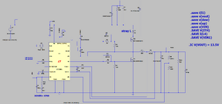
27Vin
13.5Vout
30A out.(405W)
No isolation needed.

This is too much for a Dual Synchronous Buck with each 202W Buck stage switching at 450kHz.

The synchronous Buck at high switching frequency is really meant for high duty cycle ratios
where Vin is low and Vout very low (eg 9V to 1V5). And Iout 20A or less even then.

For hard switching above a certain power level, then transformer isolated topologies become
more suitable, as the leakage reset automatically recycles the leakage current back to the input...eg in a Full Bridge.

Also, a Buck at 27Vin and 202W and 450kHz is pushing it. In the Buck, when the top FET Turns OFF, there is a lot of
energy stored in the strays of the input caps and traces, and even good layout cannot avoid this, and it creates serious
overvoltage problems on the top FET.

Would you agree this spec is not for a Dual Sync Buck at 450kHz?
 
Plenty of our customers seem to be able to make 400kHz work at these low voltages and powers - laser drilled Cu filled vias for heat transfer to sinks,

resonant gate drive, really quite narrow dead times ( 30nS ), carefully designed low capacitance chokes, 4 layer ( or 6 ) boards to steer current paths, good local de-coupling and snubbing on the Vcc in bus ( clever ) peak curr mode to keep the currents the same in each phase - we have seen 8 phase designs at 240 A out . . . buck and boost . . .
 
Thanks, even though you appear to give countenance to it, you then show that it was not done with "plain vanilla" Synchronous Buck. You
say that they used "resonant gate drive" and carefully designed low capacitance chokes. Also, that there was some form of snubbing on the Vin Bus.

Most cheap Sync Buck controllers, for example, as you know, certainly do not do "resonant gate drive".

Also, a custom designed "low capacitance" choke is of course possible....but would totally wipe out our cost budget which
can only include OffTheShelf parts.
Also, the "Cu filled" thermal vias would skyrocket the PCB cost and blow us out of the water.

I believe that rather than implement those specialist things, we would just move the frequency down to 150kHz,
and increase the damping on the gate drive....currently we are not allowed to do this, as it also slightly increases cost of the buck inductors, and of the input filter inductors.

By your answer, it does appear that you share in some degree the belief that two "plain vanilla" Synch Bucks, both at 200W and 450kHz
, and with vin from 27v and vout at 13v5, is on right on the edge of what's feasible with cheap offTheShelf parts and techniques?

Doing this as a plain vanilla synch buck is already exceeding our budget...(from findchips price checking) and so if it works, we then have to commence a marketing campaign to try and get the distys to give us real cut price deals.....As is known, the entire SMPS market of UK is owned by China. If we can't get under the price of the currently available Chinese models that do this spec with their somewhat crude but cheap "through-hole, discrete, low frequency designs", then we've had it.
 
Last edited:
Would you agree this spec is not for a Dual Sync Buck at 450kHz?

no

I don't know about 450 kHz but 20A per phase is not outrageous. It may not be the most efficient so a u-Fan is needed.
<=50 kHz is recommended for high C, low RdsOn unless GaN is SiC FETs are used.

WZ6020 controllers have generated 1kW designs.
 
Last edited:
Thanks, you possibly call for snubbing on the DC bus....by this you must surely mean an RCD clamp on the upper FET?, so that when it turns off, the stray inductive current that was going into it has got somewhere to flow.
You would think that it would be enough to have a 1uF MLCC right by the upper fet's drain as a place for that stray L current to flow, but i see your point....the snubber will likely be neeeeded due to our 450kHz, and that we just wont be able to slow the drain transitions at such high freq.......so yes, i believe we do need a RCDZ snubber for the top fet....then we will smash it off super quick without fear of overvoltage spiking it.
 
Thanks, when ON?...as you know, its the rdson...some 8millOhms or so.
By Vcc you mean the input voltage (27V for us)?.......not the "vcc" of the chip?... which is only some 5v.

In the time old way, we wish to smash the upper fet off fast, and get minimal switch loss....thus the RCDZ snubber to facilitate us in this,
in the time honoured way, as from the many days of reverse engineering.
 
and what is the resistance between the sw node and the bottom rail when the bottom mosfet is ON ?

- how much time is spent in voltage transition ? ( either way )

- what is the voltage doing in this transition time ? ( either way )

- in a classic 2 fet buck, what are the sw losses in the bottom device ( assuming a perfect internal diode ) ?

- when the top fet turns off and there is a volt spike across it - where is this spike really across if the bottom fet is on ?

- how much wood can a wood chuck, chuck, if a wood chuck could chuck wood ?

- are you seeing the situation ? . . . yet ?
 
Thanks

and what is the resistance between the sw node and the bottom rail when the bottom mosfet is ON ?........approx 6milliOhms

- how much time is spent in voltage transition ? ( either way )..........<100ns

- what is the voltage doing in this transition time ? ( either way )...........rising or falling

- in a classic 2 fet buck, what are the sw losses in the bottom device ( assuming a perfect internal diode ) ?......no sw losses in bottom fet

- when the top fet turns off and there is a volt spike across it - where is this spike really across if the bottom fet is on ?..........its across the top fet.....
--------------_____________-------------
The attached sync buck LTspice sim shows the workings of the top fet snubber.......making the vds of the top fet lower.
 

Attachments

  • TOPFET SNUB1.png
    TOPFET SNUB1.png
    98.7 KB · Views: 18
  • LTC3891_topfet snub1.zip
    2.2 KB · Views: 22
Last edited:
If you follow thru to the logical conclusion of #12 - you can make the snubber a lot simpler and less dissipative - this is what is done in GaN ckts as the high freqs make conventional snubbing problematic for heat.
 
Seeing this thread has a pause I'll step in and mention a lossless snubber which I saw somewhere among electronic-related websites. The schematic said it's for SEPIC converters but I see articles discussing it for other types of switched-coil converters.

In essence the diode (located on the primary side) steers the brief surge to the secondary side. A diode-capacitor network (almost identical) is installed across the secondary winding. This directs the 'snubbed' impulse to the output stage so that it contributes to the output stage.

Attention needs to be paid to the orientation of diode & cap. Also the orientation of secondary winding, whether it should be straightforward or swapped. Certain types of converters need to have the windings one way or the other.
 

LaTeX Commands Quick-Menu:

Similar threads

Part and Inventory Search

Welcome to EDABoard.com

Sponsor

Back
Top