Continue to Site

Welcome to EDAboard.com

Welcome to our site! EDAboard.com is an international Electronics Discussion Forum focused on EDA software, circuits, schematics, books, theory, papers, asic, pld, 8051, DSP, Network, RF, Analog Design, PCB, Service Manuals... and a whole lot more! To participate you need to register. Registration is free. Click here to register now.

Dual Switch Forward Converter - Question Help

Joined
Mar 24, 2024
Messages
1
Helped
0
Reputation
0
Reaction score
0
Trophy points
0
Activity points
15
1711314661799.png

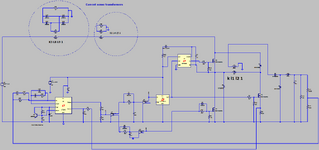
I've been told TR1 and TR2 in the picture I posed; are normally driven on simultaneously by applying a positive gate-source voltage to each of them.
As seen in the picture though; driving the lower device, TR2, directly from a low-voltage control IC connected to 0 V is relatively straightforward.
However, there is a difficulty with driving the upper device, TR1, as its source voltage swings between 0 V and 48 V. TR1 therefore cannot be driven directly from the output terminal of a low-voltage control IC connected to 0 V.
Explain how circuitry using a bootstrap diode, flying capacitor, high-voltage level-shifting MOSFET and a driver IC can be incorporated to enable TR1 to be driven from the low-voltage control circuitry.
Can anyone help me draw a diagram for this? I'm losing my mind over this question!
 
TR1 gate is referenced to its source terminal. Therefore applied bias voltage must be higher than its source terminal in order to make TR1 conduct.

As TR1 conducts it causes the join between TR1 D2 to become the same as supply voltage. Bias voltage must be that much greater. The bootstrap is a method to increase low voltage.

Simple charge pump simulation. In principle it's similar to bootstrap setup.
C2 voltage is added to supply voltage. Referred to as a voltage doubler.

charge pump clock-driven raises 6V supply to 11V at load .png

--- Updated ---

Your computer can run this simulation. Click link to:

tinyurl.com/27znxshb

1) Navigate to: Falstad.com/circuit
2) Load my schematic into the animated interactive simulator.
3) Display animation on your screen.


Toggle full screen (under File menu).

Right-Click on components to change values. Also move mouse-thumb-wheel.

If you wish you can draw your schematic similar to initial post.
 
Last edited:
Basso in his book "switch mode power supplies" has an auxiliary cct to allow bootstrapping for 2 tran forward.
It involves an auxiliary fet getting switched on for a short time just after the mains fets turn off...that refreshs the bootstrap cap.
--- Updated ---

Here is showing the kind of thing needed. (LTspice sim attached) But really, i feel if vin is around 400V then you would maybe best use a gate drive transformer.
 

Attachments

  • Two transistor forward_sense transformers.zip
    3.1 KB · Views: 31
  • Two tran forward_aux FET.png
    Two tran forward_aux FET.png
    61.4 KB · Views: 37
Last edited:

LaTeX Commands Quick-Menu:

Similar threads

Part and Inventory Search

Welcome to EDABoard.com

Sponsor

Back
Top