Continue to Site

Welcome to EDAboard.com

Welcome to our site! EDAboard.com is an international Electronics Discussion Forum focused on EDA software, circuits, schematics, books, theory, papers, asic, pld, 8051, DSP, Network, RF, Analog Design, PCB, Service Manuals... and a whole lot more! To participate you need to register. Registration is free. Click here to register now.

Diode dans resistor value for multi-MCU communication with UART

Status
Not open for further replies.

michcfr

Advanced Member level 4
Full Member level 1
Joined
Mar 7, 2012
Messages
106
Helped
0
Reputation
0
Reaction score
0
Trophy points
1,296
Activity points
2,011
Hello,
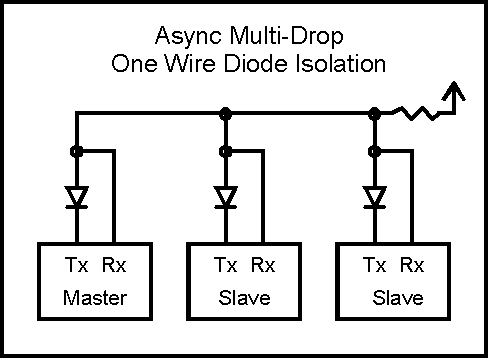
I would like to implement multi-MCU communication with UART sharing like in the picture below.
The MCU ara colocated on the same PCB and at few cm of distance; it is 3.3V logic.
What model of diode (with single or many (4 or 8 diodes) in the same package) and resistor value would you suggest?
1636828193334.png


thank you
Michel

thank you
Michel
 

I make different assumptions for bussing signals and testing choices.
Type of Diode drop at If, Schottky vs Si.
Cable capacitance by choice impedance : Worst case 100 Ohm STP
Cable length = 1m
Source impedance using Zol worst case.
Pull up Resistor.
Vol margin testing.
I did not focus on overshoot of Vol which can be eliminated by adding Rs from a 17 ohm source closer to transmission line impedance without matching at having 50% drop.

https://tinyurl.com/yh4ocpyn Falstad Simulation.
Here you will see a silicon diode with a highest Vol max margin at lower pullup current at the expense of slower rise time.

The take away conclusion is 1K may be more optimal balancing rise time duty cycle and Vol margin using be better using a schottky diode considering the Cd ESR tradeoffs of all diodes that affect Vf @ If and recovery time.

I chose a 1MHz clock.
1637010069186.png

I simulated the Vil = 1V worst case min threshold using 2V ideal logic receiver.


-ESP32: with VDD=3.3V
VIL: -0.3 - 0.25VDD
VOL: 0.1VDD and IOL=28mA (typical) with VOL=0.495V

Thus Zol= Vol/Iol= 17 Ω typ. with Vil= 1V min

-RP2040: with VDD=3.3V
VIL -0.3 0.8VDD V
VOL max 0.5V at IOL=2, 4, 8, 12mA depending on settings

Thus Zol= 250Ω, to 41.7 Ω max with Vil= 1V min

-STM32H7: with VDD=1.62V-3.6V
VIL: 0.3VDD V
VOL: max:1.3V at IOL=20mA
I don't know if it helps: The GPIOs can sink or source up to ±8 mA, and sink or source up to ±20 mA (with a relaxed VOL/VOH).

Thus Zol= 65 Ω max with Vil = 1V min
 
Last edited:

I make different assumptions for bussing signals and testing choices.
Type of Diode drop at If, Schottky vs Si.
Cable capacitance by choice impedance : Worst case 100 Ohm STP
Cable length = 1m
Source impedance using Zol worst case.
Pull up Resistor.
Vol margin testing.
I did not focus on overshoot of Vol which can be eliminated by adding Rs from a 17 ohm source closer to transmission line impedance without matching at having 50% drop.

https://tinyurl.com/yh4ocpyn Falstad Simulation.
Here you will see a silicon diode with a highest Vol max margin at lower pullup current at the expense of slower rise time.

The take away conclusion is 1K may be more optimal balancing rise time duty cycle and Vol margin using be better using a schottky diode considering the Cd ESR tradeoffs of all diodes that affect Vf @ If and recovery time.

I chose a 1MHz clock.
View attachment 172926
I simulated the Vil = 1V worst case min threshold using 2V ideal logic receiver.


-ESP32: with VDD=3.3V
VIL: -0.3 - 0.25VDD
VOL: 0.1VDD and IOL=28mA (typical) with VOL=0.495V

Thus Zol= Vol/Iol= 17 Ω typ. with Vil= 1V min

-RP2040: with VDD=3.3V
VIL -0.3 0.8VDD V
VOL max 0.5V at IOL=2, 4, 8, 12mA depending on settings

Thus Zol= 250Ω, to 41.7 Ω max with Vil= 1V min

-STM32H7: with VDD=1.62V-3.6V
VIL: 0.3VDD V
VOL: max:1.3V at IOL=20mA
I don't know if it helps: The GPIOs can sink or source up to ±8 mA, and sink or source up to ±20 mA (with a relaxed VOL/VOH).

Thus Zol= 65 Ω max with Vil = 1V min
Hello Tony,
I'm very very impressed by your work...even if I don't understand everything :)
To summarize:
-1K is a good value for the resistor
-choose a Schottky diode: 1N5712? 1N5711? BAT54? If you can please elaborate more on the prefered characteristics of the Schottky diode.

Again, thank you for your efforts


Regards,
Michel
--- Updated ---

The firmware must be able to handle half duplex anyway, specifically only send when the bus is idle.
Regarding baud rate, it must be achievable for all involved nodes. I'd probably go for a standard baud rate like 921k. At this rate, a low ohmic diode/resistor circuit should still work, e.g. 470 to 1k.
I did some tests and finally I succeed in getting open drain for TX pin (and also for RX pin) by software.
By the way, it is also possible to disable input and output and put the pin into a Hi-Z state. I don't know if it is better than open drain?
 
Last edited:

In the first order 921k is a practical limit, e.g. the highest standard UART rate supported by modern PCs and USB converters. I don't know what's available as common rate with the nodes of your design.

Secondly, there's a limit for open drain busses depending on the range and total load capacitance. You should analyze it for your application parameters.
--- Updated ---

By the way, it is also possible to disable input and output and put the pin into a Hi-Z state. I don't know if it is better than open drain?
I believe, I already answered the question. Disabling inputs however doesn't serve a purpose.

Having multiple tri-state drivers on a bus (similar to RS-485, as already mentioned) involves a risk of inadvertently enabling multiple drivers at the same time. In constrast to open drain, where it only causes data loss, it may also damage drivers.
 
Last edited:

In the first order 921k is a practical limit, e.g. the highest standard UART rate supported by modern PCs and USB converters. I don't know what's available as common rate with the nodes of your design.

Secondly, there's a limit for open drain busses depending on the range and total load capacitance. You should analyze it for your application parameters.
--- Updated ---


I believe, I already answered the question. Disabling inputs however doesn't serve a purpose.

Having multiple tri-state drivers on a bus (similar to RS-485, as already mentioned) involves a risk of inadvertently enabling multiple drivers at the same time. In constrast to open drain, where it only causes data loss, it may also damage drivers.
According to the datasheets of MCUs, the UART can go much more higher than 921k.
I think that the main constraint is about what you pointed: the open drain busses. Maybe I should complement the solution by adding a Diode for each MCU?

Concerning tri-state pin VS disable pin: I did some tests and for the moment only disabling inputs works, maybe I missed something in the code. I agree, it is more safe to tri-state the pin.
 

Hi,

to optimize LOW voltage level you could use a 74LVC1G125 as open_drain driver.
(TI datasheet)
A = GND
/OE = Tx
Y = databus

* They work from 1.7V to 5.5V,
* drive 24mA
* have low V_OL
* are fast (3.7ns)
* can tolerate up to 6.5V on any IO, even if not powered
* have high impedance output when not powered

Klaus
thank you Klaus,
Is it an alternative to the diode? still need R?
 

Hi,

it is an alternative for the diode.
and it is multidrop, means it still needs an R.
(no damage will occur when multiple nodes are active at the same time)

***
You may use the same IC as single ended push-pull driver.
Then you need function similar to RS485:
* extra microcontroller pin for driver_enable
* and the risk of problems/damage when two (or more) drivers are enabled at the same time, and thus causing high short circuit current.

According to the datasheets of MCUs, the UART can go much more higher than 921k.
I agree that every microcontroller can work higher than 921k Baud.

Just to be sur you understand the Baud rate problem correctly:
The key point is that all need to be able to work with the same frequency (wihtin tolerance). And it depends on the individual UART_clock_generators and the system clock which Baud rates are available.

Means: even if every single one may operate up to 10MBaud ... there is a good chance that the "common" frequency is below 1MHz.

Klaus
 

Hi,

it is an alternative for the diode.
and it is multidrop, means it still needs an R.
(no damage will occur when multiple nodes are active at the same time)

***
You may use the same IC as single ended push-pull driver.
Then you need function similar to RS485:
* extra microcontroller pin for driver_enable
* and the risk of problems/damage when two (or more) drivers are enabled at the same time, and thus causing high short circuit current.


I agree that every microcontroller can work higher than 921k Baud.

Just to be sur you understand the Baud rate problem correctly:
The key point is that all need to be able to work with the same frequency (wihtin tolerance). And it depends on the individual UART_clock_generators and the system clock which Baud rates are available.

Means: even if every single one may operate up to 10MBaud ... there is a good chance that the "common" frequency is below 1MHz.

Klaus
Thank you Klaus,

If you can please clarify the follwoing points:
-Value of R? 1K (as suggested by Tony) or 4.75K (no special theory behind this value, but it is an usual value for pull up at 3.3V)?
-why extra pin for driver_enable? you mean I have to use two pins on the MCU: RX and TX? extra pins to use at the MCU level?
-You said "no damage will occur..." and after "risk of problems/damage..." I don't catch the difference. If you can please explain? thx

-912K baud: ok, it is more clear
 

Value of R? 1K (as suggested by Tony) or 4.75K
As already answered several times: it depends on baud rate and trace capacitance. We can not know this.

-why extra pin for driver_enable? you mean I have to use two pins on the MCU: RX and TX? extra pins to use at the MCU level?
For push pull driver / totem pole driver you need to
* enable the driver when you want to send
* disable the driver when you don't want to send .... so other nodes can send

-You said "no damage will occur..." and after "risk of problems/damage..." I don't catch the difference. If you can please explain? thx
Two options .. divided by a space line and "***"
* the first is open drain, open collector, multi drop
* the second one is push/pull, totem pole

Klaus
 

Concerning tri-state pin VS disable pin: I did some tests and for the moment only disabling inputs works, maybe I missed something in the code.
Tristate respectively output enable for UART TX is available for most uC, probably except for those with fixed dedicated UART pin.
 

Some uC provide also configurable open drain option for TX pin.
Hello FvM,
I was just finishing the tests. This configuration works.

When one (and only one) MCU sends data:
-its RX pin: Disable input and output
-its TX pin: Output only

and for all the other MCUs:
-TX pin: output only with open-drain mode
-RX pin: Input only

Is it correct? do I have to modify something?
 

I'd use a different configuration. RX pins always enabled. TX pins switched between push-pull output and tristate/disabled output.
 

I'd use a different configuration. RX pins always enabled. TX pins switched between push-pull output and tristate/disabled output.
In my mind, RX is disabled only for the sender to avoid self receiving its own data. maybe it is not required?

I just did the test below according to your advice but it does not work:

When one (and only one) MCU sends data:
-its TX pin: GPIO_MODE_OUTPUT_OD

and for all the other MCUs:
-TX pin: GPIO_MODE_DISABLE

The only mode available are below:
-GPIO_MODE_DISABLE - disable input and output
-GPIO_MODE_INPUT - GPIO mode : input only
-GPIO_MODE_OUTPUT - GPIO mode : output only mode
-GPIO_MODE_OUTPUT_OD - GPIO mode : output only with open-drain mode
 

Hello,
Below a little wrap-up of our discussions. Can you please confirm and provide your comments. Thx

1637143663746.png
 

Hi,

looks correct.

one question: is there any possibility that one node is not powered up while other nodes need to communicate?


to your
"all other MCUs have TX pin as Open Drain-tristate/disabled ouput (disable the driver)"

just to clarify:
when a UART is idle the Tx output is HIGH. With the circuit above it causes the ´125 driver to disable.
So other nodes can send ... everyone is listening.

This is normal UART operation, thus your software does not need to do something special.

****
Rx is always listening:
This might seem to be useless when the current node is transmitting data, since it´s expected that it receives the same information as it sends out.

But the useful thing is: if by accident multiple nodes are sending at the same time .. the received data difers form the sent out data (wired AND). Thus it detects bus collisions.
Now it depends on how to react on a bus collision.
ne can expect that the receiver did get a wrong message, so it could be a good idea to automatically re-send the correct message.

It surely depends on application.

****
Often when a microcontroller is in RESET state the outputs are HIGH IMPEDANCE. This may happen because of power loss, watchdog reset, firmware update....
If in this case the communication needs to operate (other nodes), then it´s a good idea to add a pullup at the Tx output, to ensure HIGH state ... until the port is properly set up.

Klaus
 

Thank you Klaus,

-is there any possibility that one node is not powered up while other nodes need to communicate?
=> yes, one node can be in sleep mode. something to avoid?

-"all other MCUs have TX pin as Open Drain-tristate/disabled ouput (disable the driver)"
=> finally it is really necessary to do it (thanks to the ´125 driver)?

-Rx is always listening: use it as a collision detection mechanism is a very good idea. I don't know yet if I'll need it.

-pullup at the Tx output: ok
 

Hi,

=> yes, one node can be in sleep mode. something to avoid?
your "sleep mode" means: supply voltage is shut down?

If supply is shut down you need an additional circuit at the Rx side, to prevent the Rx_pin protection diodes to pull down the data line.

Klaus
 

Hi,


your "sleep mode" means: supply voltage is shut down?

If supply is shut down you need an additional circuit at the Rx side, to prevent the Rx_pin protection diodes to pull down the data line.

Klaus
Hi
The supply voltage is not shut down in sleep mode. If needed, what kind of circuit would I have to add at the RX side?

Do you have a response concerning the other question? : -"all other MCUs have TX pin as Open Drain-tristate/disabled ouput (disable the driver)" => finally it is really necessary to do it (thanks to the ´125 driver)?

thx
 

Hi,

If needed, what kind of circuit would I have to add at the RX side?
Something like an 74LVCxx gate that can accept input voltge even when supply is shut down.

Do you have a response concerning the other question? : -"all other MCUs have TX pin as Open Drain-tristate/disabled ouput (disable the driver)" => finally it is really necessary to do it (thanks to the ´125 driver)?
The ´125 is an open drain driver ... in case the microcontroller has not.
If the microcontroller already has an open drain driver built in, then - of course - you don´t need an external one.

Klaus
 

Status
Not open for further replies.

Part and Inventory Search

Welcome to EDABoard.com

Sponsor

Back
Top