Continue to Site

Welcome to EDAboard.com

Welcome to our site! EDAboard.com is an international Electronics Discussion Forum focused on EDA software, circuits, schematics, books, theory, papers, asic, pld, 8051, DSP, Network, RF, Analog Design, PCB, Service Manuals... and a whole lot more! To participate you need to register. Registration is free. Click here to register now.

Digital / Analogue grounding for DAC, ADC design?

userx2

Full Member level 3
Joined
Sep 19, 2008
Messages
173
Helped
2
Reputation
4
Reaction score
3
Trophy points
1,298
Activity points
3,067
Hello,
I am scratching my head again regarding grounding of digital and analogue parts

I have split ground planes for digital ground DGND and analogue ground AGND, joining only at the power supply regulator.

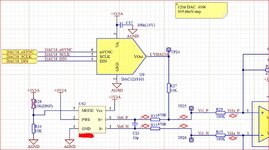
I now have a DAC DAC121S101 chip that will supply a voltage into an analogue circuit as shown.
Should that chip be grounded to DGND or AGND? I think AGND is correct since the chip supplies a precision voltage onto the analog circuit.

Datasheet: https://www.ti.com/general/docs/suppproductinfo.tsp?distId=10&gotoUrl=https://www.ti.com/lit/gpn/dac121s101

But then what about the return currents of the digital lines? They will have to cross the split ground planes.
Should I add series resistors to those? Or do I have it completely wrong?

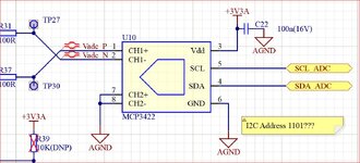
Likewise, on the other side of this circuit, I have an ADC chip MCP3422. I have the same guestion here regarding the power and grounding.
Datasheet: https://ww1.microchip.com/downloads/en/DeviceDoc/22088c.pdf

The ADC Datasheet mentions the grounding in section 3.2 but I do not understand what that means in practice.
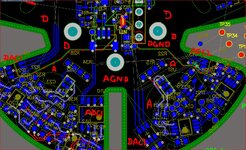
The preliminary PCB layout is also shown. The green lines show the power plane split for the AVDD but the ground plane has the same split (brown lines barely visible under green lines) This is a 4 layer PCB.
 

Attachments

  • ADC_grounding.JPG
    ADC_grounding.JPG
    116.9 KB · Views: 26
  • DAC grounding.JPG
    DAC grounding.JPG
    179.3 KB · Views: 30
  • pcb_gnd.JPG
    pcb_gnd.JPG
    348.9 KB · Views: 29
  • PSU_Ground.JPG
    PSU_Ground.JPG
    79.2 KB · Views: 31
Splitting planes this way is one of the "popular" reasons for failing EMC tests, both emission and susceptibility. As stated in your previous thread, I doubt that split planes serve a reasonable purpose in this design.
 
Hi,
I doubt that split planes serve a reasonable purpose in this design.
In my eyes: It depends.

the 12 bit resolution DAC will not be the problem at all.
Here the step size is too coarse .. and the main accuracy and precision problem will be the power supply .. here acting as V_Ref.

***
Then you have the 18 bit ADC.
What´s your focus? DC accuracy? low noise?
Give values for both.

***
Instead of talking about DGND and AGND .. maybe it´s better to think as "dirty GND" and "clean GND".

In some cases the connection between AGND and DGND is better to be located
* at the power supplies
* below the ADC / DAC

In either case I recommend to keep the "clean GND" as small and compact as possible.
(GND_plane) current flow maters, signal flow matters.

Klaus
 
Thanks FvM and Klaus.


This is not about EMC but rather about measuring low frequency signals in the higher nV and uV range.

I am just not sure what to do with this. That is despite the fact that I designed some pro audio suff in the past. It never had processors and digital stuff mixed with analogue.

In this design, I have 2 circuits. They are 2 options to try and evaluate a tiny BGA type sensor with many unknows. It is currently not clear what output, if any, can be expected from this sensor under the planned mechanical conditions.
Recommended chips, by the manufacturer of this sensor, all use a 24bit ADC and PGAs with incredible gain. Such chips are not available anywhere except China and they come with complications.

So I designed amplifiers and DAC offset compensation. Once the circuit works and is installed into the mechanics, I can tune the gain as required and hopefully a 12 bit ADC will work but if not, I have the 18bit ADC to fall back and test.

In this design, I could perhaps link the clean AGND with the dirty GND under DACs and ADCs as well as at the power supply. The return currents for the amplifiers should all back straight to the power source.

But, as FvM said, I may just be overthinking it and should just leave the ground plane solid though out the PCB.

Another consideration is that to get PCBs and assembly for this is a $4.5k exercise and I have to try factor in everything possible to try and get it to work first time.
Components are somewhat interchangeable but if I get the grounding wrong, that is bad.
 
Hi,

Correct me if I´m wrong:
* you did not set up any development goals in numbers and units (and tolerance).
* You did not do any math about the expectable errors (accuracy, precision, noise, drift ....)

If you did ... you should see which part is critical and which part is not critical.

*****
For me speaking: doing electronics design is to
* set up goals
* focus on the goals
* do the math on how the goals are influenced by expectable errors
* choose circuits according the math
* choose devices according the math
* iterate to do improvements, starting with improving the most erroneous part of the circuit.

For sure you are free to go your own way.

Klaus
 
Placement of the components is the most important factor (in any PCB design).

I would start of with a split ground to aid placement, no signals to cross on to the wrong ground. Then decide whether to have a split ground plane or not...
 
Hi,

Correct me if I´m wrong:
* you did not set up any development goals in numbers and units (and tolerance).
* You did not do any math about the expectable errors (accuracy, precision, noise, drift ....)

If you did ... you should see which part is critical and which part is not critical.

*****
For me speaking: doing electronics design is to
* set up goals
* focus on the goals
* do the math on how the goals are influenced by expectable errors
* choose circuits according the math
* choose devices according the math
* iterate to do improvements, starting with improving the most erroneous part of the circuit.

For sure you are free to go your own way.

Klaus
Hi Klaus, but then you would probably not be able to design this circuit since there are too many unknows for your method to even get started.
Only doable math has been done in this case.
And how would any math sort out the potential grounding issues?

Best regards
X
 
Hi,
Hi Klaus, but then you would probably not be able to design this circuit since there are too many unknows for your method to even get started.
I´m a professional high precision electronics designer for decades now.
I guess I´ve experienced a lot of difficulties .. and I´ve solved a lot of them.

Decades ago for example I`ve designed an X-Ray meter with 2Ch, 10kSmpl/s ... with a resolution down to 7pA ... and a trigger at 30pA. I had almost no specification about sensors ... and algorithm. And especially when there is a lack of information one needs to investigate about the physical limits.
Doing a lot of tests and math ... to find out wich part of the circuit is critical.

From my experience I can say I never had a fully specified task from the beginning. It always is part of the designer to make the specifications complete.

Only doable math has been done in this case.
OK. Shakespeare said: well roared, lion.
Then prove me wrong with my opinion, that the drift of the power supply voltage of your circuit overrules the expectable grounding errors by several decades. I guess this is (one of) the biggest error source in your circuit, indeed I expect the errors caused by power supply noise and drift maybe to be higher than your entire "sensor measurement signal range". It may be higher than OPAMP errors, noise errors, offset drift errors and ADC errors combined.

I did not do the math .. but you said you did! So it should be simple to show. Or at least an estimation.

And how would any math sort out the potential grounding issues?
This is exactly the problem. You don´t see that the grounding issue is no issue at all in your system ... because other errors are way bigger.
No need to sort out a problem that does not exist.
Just look at the results of your math. They show you.

Do you know that independent errors add by using squares?
Do you also know what this mathematically means?
An example: Let´s say you have three error sources: The one introduces 30mV, the other 5mV and the other 3mV.
So the total expectable error is: 30.5mV
You may do handstands on the 5mV and 3mV errors, you may invest hours, weeks of discussion ...
and even if you manage to reduce both of them to 1/10th ie, 0.5mV and 0.3mV ... you still have about no improvement. It still will be about 30mV of error.
But if you reduce the 30mV error by a tiny bit only ... down to 29.4mV (just by 0.6mV)... it already overrules all effort to reduce the other two errors.
Do you understand that it´s much easier to reduce the error of 30mV down to 29.4mV (reduced by 2%) than to reduce 5mV down to 0.5mV (reduced by 90%)?
It´s better to reduce the one by 0.6mV than reducing the other by 5mV. You just need to focus on the bigger one. That´s what science tells.

This mathematically shows it has no significant impact on performance to reduce the smaller errors even more.
This example uses just a ratio of 1/6 ( 30mV vs 5mV) .. in your circuit I expect the ratio to be much bigger ... making things worse.

I know there are people who ignore physics and math ..
Their goal is to reach the north pole .. but they decided to go along the equator. And nobody is allowed to tell them to change their direction. They want to talk about speed, gravitation and everything else. They don´t want to rethink their decision... or follow rules of physics and math. They go their way.

It´s your job, it´s your effort, it´s your application ... My post is a just well meant "recommendation" .. nothing more. Like a map showing the path.
Still it´s your choice which direction to go.

Klaus
 
Hi,

regarding your "analog" 3.3 V regulator. I would recommend to connect its ground at least to the "non-dirty" analog GND plane, as the LDO will regulate its output with respect to its GND pin. This of course depends wheer you will tie AGND and DGND together.

BR
 
The error analysis is complicated, eg. when do you use statistical methods of
summing error versus straight linear summation ?

The root sum of squares carries a requirement the error sources be uncorrelated.
Typically that is not always the case, just look at (for your part) the curves of
Vos and PGA G versus T, strong correlation as you can see. Also the application
of statistical analysis is best served on data sets, the larger the better (typically).
Additionally we have the problem that root sum of squares makes our system "look
better" than it is, worst case. Eg. has been used by engineering and marketing to
convey a better design than actually is when trying to make measurements. After
all statistical analysis still gives one the probability that simple sums of error will
occur with some non zero probability.

So what is worst case ? Simple sum or root sum of squares ?

Not a mathematician here. You have ,to decide which method makes most sense
in your design. I think "real" 12 bit absolute error performance is not trivial over T
and V, even if you start with 16+ bit converters. And then we have real noise, one
would jump on root sum of squares until one considers, is it uncorrelated in a
mixed signal system full of clocks and other deterministic processes.....


Regards, Dana.
 

LaTeX Commands Quick-Menu:

Similar threads

Part and Inventory Search

Welcome to EDABoard.com

Sponsor

Back
Top