Continue to Site

Welcome to EDAboard.com

Welcome to our site! EDAboard.com is an international Electronics Discussion Forum focused on EDA software, circuits, schematics, books, theory, papers, asic, pld, 8051, DSP, Network, RF, Analog Design, PCB, Service Manuals... and a whole lot more! To participate you need to register. Registration is free. Click here to register now.

CST and/or HFSS software to design LPDA

alftel

Member level 1
Member level 1
Joined
Apr 21, 2019
Messages
38
Helped
4
Reputation
8
Reaction score
5
Trophy points
8
Visit site
Activity points
517
Hello guys (and gals),

I wonder what it will take money wise to task any of you who owns or have an access to licensed CST and HFSS software to design, simulate/adjust Log Periodic Dipole Array (LPDA) antenna based on our specification, such as maximum size, Err and frequency range. We can provide a preliminary "good guess" measurements to start from. Teflon material, 1.52mm, rated to 10 GHz, 1oz ENIG finishing.

Cheers,
Alex
 
Last edited by a moderator:
Solution
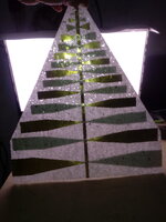
I know this article (the one that you did show picture from) - we attempted to replicate this design in a past in order to see if it does work. I can tell you right now that design as it explained in this article just does not work and there is no way it would demonstrate S11 and SWR as claimed in this article. I think bowtie dipoles that supposed to help to "cover" lower end need to be a "normal" printed bowtie style - i.e. solid triangles. This is why we do need a solid simulation to begin with, size allowance should be sufficient
--- Updated ---

This is what we did in a past - 300-8000 MHz LPDA crafted with FR4, 1.6mm substrate. We usually follow our good friend Kent Britain advice posted here...
Using a Bow-tie element in a LPD antenna doesn't help reducing the size of the structure, because bow-tie length (between its extremities) is still λ/2 as in a normal half-wave dipole.
But the bow-tie element will improve the LPD efficiency at lower frequencies.
 

Attachments

  • bow-tie lpd.jpg
    bow-tie lpd.jpg
    74.1 KB · Views: 154
I know this article (the one that you did show picture from) - we attempted to replicate this design in a past in order to see if it does work. I can tell you right now that design as it explained in this article just does not work and there is no way it would demonstrate S11 and SWR as claimed in this article. I think bowtie dipoles that supposed to help to "cover" lower end need to be a "normal" printed bowtie style - i.e. solid triangles. This is why we do need a solid simulation to begin with, size allowance should be sufficient
--- Updated ---

This is what we did in a past - 300-8000 MHz LPDA crafted with FR4, 1.6mm substrate. We usually follow our good friend Kent Britain advice posted here: https://www.wa5vjb.com/references/DesigningPCB-LPs.pdf and while it is an "approximate" approach it does require a number of tries with adjustments etc. etc. Teflon material is expensive, so we would like to start with well done simulation first in order to minimize adjustments efforts.

1699376853267.png
 
Last edited:
Solution
You are right, the bow-tie elements should be solid triangles, due to the surface currents distribution.
YUP , BOW TIEs (band width) with careful taper and straight wherever possible (Gain) In MY experience...smooth Z curves at 50 ohms all the way from 400MHZ to 6ghz (could be made higher easily) UNDER 400 mhz...seems like you need a METAL FRAME lpda
(around a meter or more)...to get some energy on those long wavelenght...
Captura.PNG
 
I know this article (the one that you did show picture from) - we attempted to replicate this design in a past in order to see if it does work. I can tell you right now that design as it explained in this article just does not work and there is no way it would demonstrate S11 and SWR as claimed in this article. I think bowtie dipoles that supposed to help to "cover" lower end need to be a "normal" printed bowtie style - i.e. solid triangles. This is why we do need a solid simulation to begin with, size allowance should be sufficient
--- Updated ---

This is what we did in a past - 300-8000 MHz LPDA crafted with FR4, 1.6mm substrate. We usually follow our good friend Kent Britain advice posted here: https://www.wa5vjb.com/references/DesigningPCB-LPs.pdf and while it is an "approximate" approach it does require a number of tries with adjustments etc. etc. Teflon material is expensive, so we would like to start with well done simulation first in order to minimize adjustments efforts.

View attachment 186086
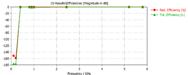
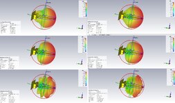
LOTS of losses (Dielectric losses add up to some 10-20 % at some frequencies ) , little to no energy (efficiency suffers highly mostly seen on RX sensitivity , good Gain and directivity ,tho
 
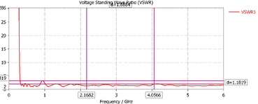
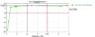
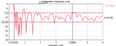
Optimized from 300mhz to 6ghz FLAT Z ,HIGH EFFICIENCY (PES dielectric) moderate gain (reflector could be added) under 2 VSWR...37 by 42 cm...
 

Attachments

  • 1.PNG
    1.PNG
    55.4 KB · Views: 61
  • 2.PNG
    2.PNG
    56.8 KB · Views: 58
  • 3.PNG
    3.PNG
    52.7 KB · Views: 57
  • Captura.PNG
    Captura.PNG
    69.5 KB · Views: 59

LaTeX Commands Quick-Menu:

Similar threads

Part and Inventory Search

Welcome to EDABoard.com

Sponsor

Back
Top