Continue to Site

Welcome to EDAboard.com

Welcome to our site! EDAboard.com is an international Electronics Discussion Forum focused on EDA software, circuits, schematics, books, theory, papers, asic, pld, 8051, DSP, Network, RF, Analog Design, PCB, Service Manuals... and a whole lot more! To participate you need to register. Registration is free. Click here to register now.

Constant Current Super Capacitor Bank

Status
Not open for further replies.

adnan012

Advanced Member level 1
Joined
Oct 6, 2006
Messages
468
Helped
2
Reputation
4
Reaction score
2
Trophy points
1,298
Visit site
Activity points
4,923
Hi,

I am working on a super-capacitor bank charger. The specs are

Super Capacitor Bank 100F/15V
Charging time required 60 seconds
Input voltage 18V
Max Charging voltage 15V

I am using a synchronous buck with constant current (maximum) loop + CV loop. At startup the charging current is 40A. As the capacitor voltage start rising the charging current starts decreasing. After 60 seconds the 15V at capacitor bank is achieved, at this point current maximum current was 20A. its decreases from 40A to 20A linearly. At startup the PWM on time at high side MOSFET gate is very small and it starts growing as the charge builds up on the capacitor.

I want to know why the current does not stay at 40A through out the charging process. All temperatures are in limits.

Best Regards
 

Hi,

Sure, what else did you expect?
Did you read the datasheet, post#10 (especially 2nd line) and post#12?

Klaus
 

    adnan012

    Points: 2
    Helpful Answer Positive Rating
Thanks for reply .

Could you please make a sketch, so that i can implement it correctly.
--- Updated ---

Hi,

Sure, what else did you expect?
Did you read the datasheet, post#10 (especially 2nd line) and post#12?

Klaus
In worst case, do you think I need some sort of slope compensation? Is it applicable in this design?
 
Last edited:

I think, the const U/const I scheme can work, although I'm still missing an English EG1163 datasheet. I rather expect that SDHIN or SDLIN are becoming active at higher output voltage due to increasing current ripple.
 

Thanks for reply .

This is what i understand from your previous post.

I have disabled the SDHIN and SDLIN pins using copper piece.

Now Vin = 17.5V

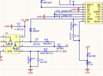
from Vout = 0 to Vout 12.5 or 13.2 i can charge at constant current (17A) .After this the current drops quickly. The PWM at high side switch looks strange . one cycle long and one cyce short (duty cycle).
 

Attachments

  • 1.PNG
    1.PNG
    40.9 KB · Views: 225

Hi,

Your shown circuit is inclomplete. I see many supply voltages:
* VBatt: What voltage range is? Is it stable and reliable?
* VCC: What voltage range is? Is it stable and reliable?
* +12V: What voltage range is? Is it stable and reliable?
* 5V Ref: What voltage range is? Is it stable and reliable?
We can´t see where they come from / how they are generated.... how precise they are...


I can´t remenber where I wrote to disconnet FB at all.

1) disconnect R19. Just desolder it. Nothing more.
2) follows..

Klaus
--- Updated ---

Thanks for reply .

All voltage levels are with in range and are stable.

Input is 17.5 V

I just removed the voltage feedback resistor .Rest of the components are still there .

I will share scope shoots tomarrow.

Regards
 

I think, the const U/const I scheme can work, although I'm still missing an English EG1163 datasheet. I rather expect that SDHIN or SDLIN are becoming active at higher output voltage due to increasing current ripple.
Without an english datasheet or some scope captures, I don't think there's much we can do here. The way the OP has SDHIN and SDLIN connected is different than what the datasheet shows, but without the datasheet I have no clue what those pins are even meant for.
 

Thanks for reply.

SDHIN and SDLIN provides maximum current limit. I can disable this feature.
The max duty cycle that can be achieved is 93%.

Regards
 

SDHIN and SDLIN provides maximum current limit. I can disable this feature.
It's a very strange implementation though. No idea why you'd want and independent current limit for each FET....

Anyways, your R11 gives a peak current limit of 36A. The average current limit will be 36 - Ipp/2, where Ipp is the peak-to-peak inductor ripple current. Initially when the cap voltage Vcap is near zero, duty cycle will be near zero which means ripple is also very small. As Vcap rises, so must duty cycle and ripple, meaning the effective output current limit will fall. In theory, Ipp will be maximum at 50% duty cycle. If you switching frequency is 20kHz and the inductance is 47uH, and Vin=18V, then the max Ipp would be 4.8A, so that won't affect the max output current very much. All of this is aside from your separate current regulation loop (which only looks at average current).

However, if the inductor starts to saturate, then the max Ipp could be far higher. That's why I initially asked about inductor saturation.
 

Something really odd is going on here.....
Just as an experiment, try temporarily replacing the lower mosfet with a Shottky diode, and see what happens.

Its not often realised, but an active buck converter can become bi directional !
If you try using an active buck converter to charge a battery for example, its possible for current through the choke to reverse, and the whole contraption back feeds power in boost mode, from the the battery load, back to the power source.

So you need to be very careful about duty cycle control, and the in/out voltage differentials.
None of this can happen with the usual more common resistive load, and active buck regulators will work exactly as expected.
With a battery or an ultra capacitor load, there may be unexpected issues.

Replacing the active diode with a real passive diode, eliminates the possibility of current reversal in the choke.
That removes any restriction on duty cycle, and the control loop can then do it's thing without interference.

That is obviously not a satisfactory final solution. But if the whole thing then behaves itself, it might assist with understanding the actual mode of operation, which might be rather different than anticipated.

For a very high power circuit, it may be more practical to just monitor choke current with a Hall sensor, and make absolutely certain the choke current never reverses.

This is only a theory, based on some of my own past frustrations.
The actual cause may eventually prove to be something completely different.
 
Status
Not open for further replies.

Similar threads

Part and Inventory Search

Welcome to EDABoard.com

Sponsor

Back
Top