I simulated the Mosfet circuit with try and error method and draw real part of input impedance vs frequency but I did not get the desired response yet (it isnt negarive and is positive for all frequency)
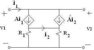
It seems this circuit doesn't work as a NIC, probably because the additional currents needed to create the correct reference points (i.e. due to the multiple current mirroring). I must admit I didn't know in the very beginning of this thread that you need a NIC circuit.
I tried the circuit with supposed technology currents and Kp values for your process and a DC input current of 10mA (it works between 1..100mA).
To get reasonable operation points, I had to scale up your resistor values by a factor of 1000 (and still had to use ridiculous large MOSFET widths), s. this PDF: View attachment CCCS3.pdf
With the given DC input current of 10mA, the pos. input impedance is 7.7Ω .