electronicman26
Full Member level 2

Hello
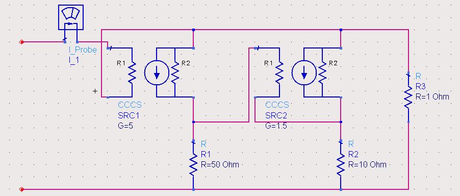
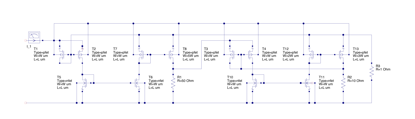
I simulated this circuit schematic with ADS, R1 is 0 ohm and R2 is inf, now I want to replace ideal model of CCCS with circuitary model of CCCS, how is it possible?
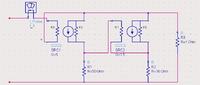
I simulated this circuit schematic with ADS, R1 is 0 ohm and R2 is inf, now I want to replace ideal model of CCCS with circuitary model of CCCS, how is it possible?

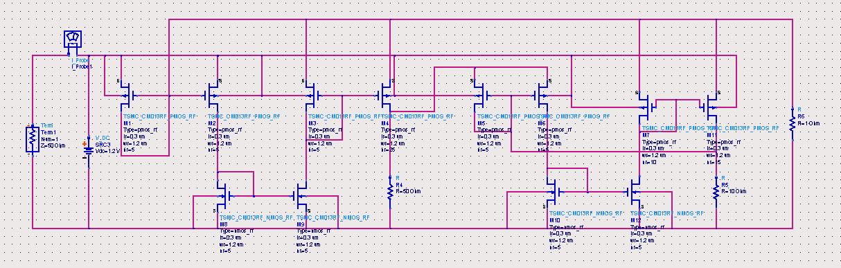

 but you have exprince, I would be glad you give me good estimation