Continue to Site

Welcome to EDAboard.com

Welcome to our site! EDAboard.com is an international Electronics Discussion Forum focused on EDA software, circuits, schematics, books, theory, papers, asic, pld, 8051, DSP, Network, RF, Analog Design, PCB, Service Manuals... and a whole lot more! To participate you need to register. Registration is free. Click here to register now.

Buffer hardware between oscilloscope probe and sound card line in

Status
Not open for further replies.
Nicely explained Jason - thanks.

So essentially any voltage value on the negative opamp input less than what is on the positive opamp input and the opamp acts as an amplifier.
And as far as I can gather they do this by converting some of negative voltage supply to positive voltage and adding it to the output.
 

So essentially any voltage value on the negative opamp input less than what is on the positive opamp input and the opamp acts as an amplifier.
And as far as I can gather they do this by converting some of negative voltage supply to positive voltage and adding it to the output.

An op amp with negative feedback seeks to set the negative and positive inputs to basically equal values (+/- a few microvolts depending mainly on the op amps open loop gain) by adjusting its output, so in this case it acts as an amp by adjusting its output so that the voltage at the point between R4 and R5 becomes the same as the voltage at the positive input. When S1 is open the output must be the same as the positive input to achieve this. When S1 is closed the output must be 10x the positive input to achieve this.

It does not convert voltage polarity or add voltages. Fundamentally, it just uses transistors to control how much of the supply current is passed through the output, based on the difference between the positive and negative inputs (but with an enormous gain, e.g. 100,000x or more - not generally useful without the negative feedback). The output draws from the op amps supply, not its inputs - thats part of why they can be used as buffers between mismatched impedance circuits. The output can never be greater than the op amp supplies, it is clipped near the rails (exactly how close to the rails the output can go depends on the op amp and is listed in the datasheet). I think the tl082 only goes +/- 12v worst case output, I'm pretty sure it's not rail to rail, so in x10 amp mode with a +/-12v supply input signals > slightly under 1.2v will clip to the max output range (you'd need slightly more than +/-12v supply rails for the tl082 to hit a full +/-12v output range). There are plenty of op amps with a wider output voltage, but none will output beyond the supply voltage.

See the other pages on that op amp link I posted they have lots of good info about how they work, its well written and concise.

J
 
Last edited:

OK.

But what is the basic mechanism that results in the increased current flow ending up as increased voltage at the output?

I am familiar with how a transformer works but clearly an opamp does not contain a transformer.

Transistors amplify current flow.

I was assuming that the voltage amplification was in some way similar with what happens in a AC to DC rectifier with filter where by the negative part of the cycle is stored in a capacitor which is then discharged in the gaps in the positive cycle after the rectifier.
 

First, read this! It is a quick and easy read and will give you a much greater understanding.

--

Op amp output stage are typically a **broken link removed**.

Here I've created a simulation of a push pull emitter follower in Falstad's simulator, clicking the link will cause a Java applet to open with an animated simulation. Use the slider labelled "control" on the right to adjust the control voltage. Scopes on bottom show output current and voltage: http://tinyurl.com/bom2kqo

--

Also of interest:
- A very basic internal circuit diagram of an op amp.
- A circuit diagram of an LM741.

--

J
 

Thanks for the info - will read through it. I was actually trying to gain some understanding of how the opamp internally increases the voltage rather than what it does when you attach resistors etc to it in a certain way.
Perhaps the way it acheives it is more along these lines: http://users.tpg.com.au/users/ldbutler/TransisVoltAmp.htm?

I have just found some other info about opamps where they convert a square wave input to triangle or saw tooth which means I can't use one to amplify a 555 single before it goes into the gate of a mosfet.

I actually wired up a non-inverting amplifier on my bread board and passed the 555 output through a transistor totem pole and then on through the non-inverting amplifier and it doesn't work. It wont drive my tv flyback transformer. And given the above info I can understand why.

So I am going to have a go at this: http://users.tpg.com.au/users/ldbutler/TransisVoltAmp.htm.

Will see if modifying my transistor totem pole along these lines will do the trick.

I also started reading about an interigator where you replace one of the resistors of a non-inverting amplifier with a capacitor and that it is used in audio circuits, which is along the same lines as a square wave.

But I have pulled a 2 channel amplifier chip off a stereo circuit board. It is a fairly simple affair by the datasheet. Could try that with my 555 square wave as well. Might save me frigging around with adding capacitors to a non-inverting amplifier.


In the circuit I am fiddling around with I have added a voltage divider to reduce the 555 output voltage to just below 5V, the maximum Vbe of the BD140 and BD139 I am using.

And it seems to be the case, from DMM measurements, that Vbe determines the voltage across the collector-emitter no matter what voltage you have the collector of the BD139 connected to. Funny but I haven't found a website yet that explicitly states this.

The problem is that the threshold of a FET is around 4V and 5V is a little close to it. I have read else where that running a FET at near threshold causes it to have high resistance to source drain current and that you need at least 10V on its gate to turn it fully on.

FET gate drivers have been suggested but it is a matter of knowing which type to get and finding a local source of them.
 

BS981 & BSR83

These are mosfet gate driver ICs that are available at my local Jaycar.

Do you know where I can find the datasheets for these?

A google search reveals a whole lot of irrelevant crap and the Jaycar national website does not even list them.
 

ATX Pin 14
−12 V

It's on the ATX but if he's trying to make a device that uses only standard connections to the computer there's no negative outs aside from tapping into the motherboard connector - but if that's not an issue then yeah. SATA gives +3.3/+5/+12, IDE gives +5/+12, fans are +12. You could get -5/0/+7 from the IDE connector but then it's not directly compatible with the sound card input and it limits the signal range more.

- - - Updated - - -

Although the PCI bus has a -12V supply, I guess you could put the circuitry on a pci protoboard and tap into it that way if you wanted to sacrifice a slot (of course this all assumes a desktop host, laptops these days pretty much only have usb and esata power out, commonly).
 

buff.gif


If I was to place a diode voltage clamper at RCA (to ensure the voltage output to the sound card does not exceed 2.1V no matter what you do with S1 and R6, i.e. 3 x signal diodes in series and then two sets of these in inverse parallel, then is a resistor between the series diodes and ground recommended or not? Or do the series diodes dissipate enough power by themselves?
 

Another issue that has just occured to me with the output of this buffer circuit.

The author states that the output is always less than 12V but most sound card line in sockets have a maximum of 2V.

So I would really need a diode voltage clamp on the output of the opamp.

If it was 2 sets of 3 series diodes in reverse parallel then the peak voltage output would be clamped +2.1V and -2.1V (3 x 0.7V). But the voltage swing between the extremes would be 4.2V.

So what does the maximum 2V sound card line in limit refer to? The voltage swing or just the voltage peaks.

I am wondering if I actually need to clamp the peak voltage output to 1.4V (2 x 0.7V) so that the voltage swing is 2.8V (at least much closer to the 2V limit for sound cards)
 

boylesg said:
So what does the maximum 2V sound card line in limit refer to? The voltage swing or just the voltage peaks.

>= 2V peak (4V p-p) would make sense for pro audio equipment levels, 1V peak would not. These guys limit it to 3. Give your circuit a ~100-600Ω minimum output impedance (pro line level specs are given at 600Ω iirc).

I found this part Semtech RCLAMP2502L (Digikey ~$2) that seems perfect for the job. Use the differential protection configuration outlined on pages 5-6 of the datasheet (where your signal is one line and ground is the other, leaving pins 2,3,6,7 unconnected).

E.g. your final output stage (very final; after that last pot in the most recent circuit you posted) would be:


Include the 600Ω resistor (or whatever) to set minimum output impedance if necessary.

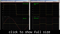
Which clips the output like this (pspice using the spice parameters from the datasheet, red = unclipped, yellow = clipped, sim with 600Ω output, 10kΩ soundcard input):


That TVS is designed for high speed data line protection and the diodes have very low capacitance. Freq/phase response is flat (≈ -0.0038 dB, -0.04° @ 96kHz). Note that you will start to see signal distortion as your signal approaches bv, the significance of which depends on your requirements, so pick a max acceptable value in software and values above that can be reported to the user as clipped.

Also the 2502 has 24A continuous limit and 40A surge limit, you'll blow a lot of other stuff up before you burn up this diode, so no, no additional ground resistors necessary.
 
Last edited:

Status
Not open for further replies.

Part and Inventory Search

Welcome to EDABoard.com

Sponsor

Back
Top