Continue to Site

Welcome to EDAboard.com

Welcome to our site! EDAboard.com is an international Electronics Discussion Forum focused on EDA software, circuits, schematics, books, theory, papers, asic, pld, 8051, DSP, Network, RF, Analog Design, PCB, Service Manuals... and a whole lot more! To participate you need to register. Registration is free. Click here to register now.

Bubba Oscillator and THD

Status
Not open for further replies.
LvW: Could you please send me the rough schematic of two integrator based oscillator because this would be a great exercise for my brain also. If I could not solve it my self I am gonna ask you WHY? So be prepared.

:)
 

Hi LvW,

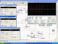
Today's modification yielded some improvement. See the below image.


Can you give some explanations to the figure provided? What is the main subject to watch?
 

I meant to say that distortion figure has came down from 0.010% to near around 0.001% at 2KHz. Only to get your opinion how can I improve further. I am sorry if I am disturbing you.
 

But you didn't tell what has been changed to achieve this.
 

I meant to say that distortion figure has came down from 0.010% to near around 0.001% at 2KHz. Only to get your opinion how can I improve further. I am sorry if I am disturbing you.

I suggest to be very cautius with THD simulation results - and, more than that, I doubt if it is possible to realize RC oscillator hardware circuits with a THD around 0.001% (or even lower) without special regulation circuitry.
 

Actually I made the RC values like the following while playing and got the THD shown above

1st Section: R=2K5, C=80nF
2nd Section: R=5K, C=40nF
3rd Section: R=10K, C=20nF
4th Section: R=20K, C=10nF

Yes physical circuit will have totally different THD figures (real one). Can I use VCA810, SSM2018 or LT1228 as regulation circuitry?
 

Can I use VCA810, SSM2018 or LT1228 as regulation circuitry?
Any variable resistor or VCA of good linearity can be used as a variable gain element for an amplitude controller. I would prefer a linearized FET variable resistor.

In my understanding, the total THD is given by the distortion created in the dedicated clipping stage (the stage with highest amplitude) and the low pass characteristic of succeeding RC stages. In addition, the surplus loop gain and the clipping charateristic are affecting the initial clipping stage THD. Also excess nonlinearity of involved OPs can make an impact.

Considering this situation, I don't see how adjusting the RC dimensioning could improve overall THD, except for modifying the loop gain, and possibly affecting additional distortions by optimizing the load for the OPs. But it may be a simulation artefact as well.

It is a type of phase shift oscillator with 45 degree phase shift for each section. which is reason why we can get very low frequency drift
I fear, your statement explains nothing.
 

Hi FvM,

When I put above RC configuration in reverse order THD goes high. Well I think there is some link between THD and RC loading (impedance) effects. BTW, which JFET do you suggest for this work 2N5486 and Jxxx series is available in the local market over here.

Is this topology correct ?
AC to DC converter (RMS Value) ---> Differential Amplifier (IN1=RMS Value, IN2=Vref) ---> JFET (As Variable Resistance)
 

When I put above RC configuration in reverse order THD goes high.
How about using the highest R uniformly?
which JFET do you suggest for this work
Highest Up gives best linearity. In addition the gain part set by the FET should be small. At best, a series resistor reduces the voltage across the FET. Usual cancellation of quadratic term by a voltage divider, as shown in all application examples should be applied.
Is this topology correct ?
The amplifier should preferably implement a PI characteristic.
 

Following were the results of different RC configurations

THD 0.327%
=========
Section-01 R=20K C=10nF
Section-02 R=20K C=10nF
Section-03 R=20K C=10nF
Section-04 R=20K C=10nF

THD 0.01%
========
Section-01 R=20K C=10nF
Section-02 R=10K C=20nF
Section-03 R=20K C=10nF
Section-04 R=10K C=20nF

THD 0.002%-0.001% or lower
======================
Section-01 R=2K5 C=80nF
Section-02 R=5K C=40nF
Section-03 R=10K C=20nF
Section-04 R=20K C=10nF

THD 0.386%
=========
Section-01 R=20K C=10nF
Section-02 R=10K C=20nF
Section-03 R=5K C=40nF
Section-04 R=2K5 C=80nF

Do you use LTSpice ? If yes, then please have a look on AGC part which I drawn today but with wien-bridge. Output node is V(17).

Please rename the extension from txt to cir.
 

Attachments

  • Wien_AGC.txt
    2 KB · Views: 66

Sameer,
from theory, I am afraid there are no explanations for the severe differences in THD "measurements".
But - as I told you already: Don`t blindly trust THD simulations. I don`t now how THD is calculated in LTSpice.

Why don`t you post a circuit dagram for AGC?
 

I don't find it convenient to read netlists. But apparently, there's no linearization network at the FET gate.
 

Hi LvW and FvM,

One thing I must clear "I also do not trust simulation THD figures". THD simulation only helps me finding factors which affects distortion. I am not an electronics expert so I tweak component values and see how they impact THD figures. These points can help a lot while building practical circuit. Please correct me If I am wrong. I am treating both of you as my instructor (teacher).

Sure, I'll post the circuit diagram once I'll get back to home. Currently I am at workplace.

FvM could you please post some examples of linearization network.
 

FvM could you please post some examples of linearization network.
https://www.edaboard.com/threads/129234/
THD simulation only helps me finding factors which affects distortion.
Using simulation to evaluate principle effects rather than expecting an exact reproduction of a real circuit is a reasonable viewpoint. A problem arises, if you can't be sure if the observed effects are due to principle circuit behaviour or possibly simulation artefacts, e.g caused by numerical truncation or imperfect models. To prove, that the simulation is correct, you should either check the result in a real circuit, or find an explanation based on specified component properties.
 
Last edited:
Sameer, I have one question regarding the gain stage:
In your circuit diagram I see a variable resistor (pot) to set a gain of app. G=4.
Question: What is the actual gain value? I suppose, you know that it should be only slightly larger than G=4 in order to keep the amplitude limitation effect as small as possible?

---------- Post added at 10:14 ---------- Previous post was at 10:01 ----------

The above applies also in case you introduce AGC regulation with a FET. The occupied dynamic range of the regulation circuitry should be as small as possible (only very small gain variation) - otherwise the non-linear element (FET) introduces additional distortions.


Nice thread. :)

A problem arises, if you can't be sure if the observed effects are due to principle circuit behaviour or possibly simulation artefacts, e.g caused by numerical truncation or imperfect models.

I got your point.

Question: What is the actual gain value? I suppose, you know that it should be only slightly larger than G=4 in order to keep the amplitude limitation effect as small as possible?

Yes, It is slightly larger than 4.
Pot is set at the point (around 40% of 10K) where oscillation remain steady further 0.1% (10 Ohm) reduction in pot resistance (10K) results start of amplitude decay.
 

Nice thread. :)

OK, fine that you`ve found this thread. So you can learn everything that`s necessary to use FET controlled gain.

---------- Post added at 13:16 ---------- Previous post was at 13:13 ----------

Another question: Sameer, is there no requirement to vary resp. tune the frequency of your oscillator?
 

Another question: Sameer, is there no requirement to vary resp. tune the frequency of your oscillator?

Sorry, I could not understand.

Do you mean Frequency variation vs Gain variation ?
 

Status
Not open for further replies.

Part and Inventory Search

Welcome to EDABoard.com

Sponsor

Back
Top