Continue to Site

Welcome to EDAboard.com

Welcome to our site! EDAboard.com is an international Electronics Discussion Forum focused on EDA software, circuits, schematics, books, theory, papers, asic, pld, 8051, DSP, Network, RF, Analog Design, PCB, Service Manuals... and a whole lot more! To participate you need to register. Registration is free. Click here to register now.

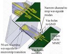
Bond wire application at 145 GHz.

Status
Not open for further replies.
Something simulator related. When simulating patches very close to another meshed layer (for example small local ground), things can go wrong.

When you simulate a small horizontal rectangle above a non-meshed (infinite) ground plane layer, results are mostly good, even if the distance to ground < mesh size of rectangle. However when the ground is just another metallic layer that needs to meshed, thing can go complety wrong. From my experience with old versions of IE3D, results are fine if the mesh size << distance between structures, or the mesh of the rectangle should be aligned with the mesh in the meshed ground layer. I suppose it will be the same in HFSS and other MoM based simulators.

If came across this when simulating some planar resonating structures that had small local (floating) ground layers that needed to be meshed also.

Wire diameter: Is your wire diameter in the image properly scaled, or is it much smaller in reality or in your simulation? Diameter affects characteristic impedance of your CPW bond wire structure.
 
well, unfortunately you are screwed, in a technical sense.

The bond wires are going to behave roughly as inductors. The proper way to match this series inductance is with a shunt capacitance on either side. this can provide a good 50 ohm match, but also forms a lowpass filter--probably with a cutoff frequency above 145 GHz.

You can try to bandpass resonate the series inductance of the bond wire...but that will have a fixed bandwidth.

You also could try to raise the characteristic impedance of the system.....a given fixed inductance value would have less detrimental effect if Z0=150 ohms, for instance.
 
They have inductance, but there is also capacitance between the signal wires and the return wires, so there is a characteristic impedance (that one can find with ATLC, or via EM simulation).

I agree with raising the system impedance as Zc of the wire structure will be certainly more then 100 Ohms. Given the blue structure (ground is 5 um below thin trace) there may be some limitations.
 
well, in reality u do not know the distance accurately (for these wavelengths) of the spacing. Also if you have two parallel bond wires connected to the same pads, they do not necessarily have the same potential along their length, as they are not connected at midpoint, for instance.

How about instead of bond wires, some sort of flip chip rf board material pressing down, with coplanar lines on it and solder bump attach? Maybe copper ribbons printed on kapton?
 
@biff44: besides accuracy issues, it still remains a transmission line (with common mode to differential mode conversion and vice versa). There is symmetry (each signal wire is left and right of the symmetry plane), so I don't expect large current unbalance in the signal bond wires. I assume that when this is for a serious application there will be some trimming to do final matching.

I fully understand that ribbon or other planar structure would be better, but very likely he cannot or will not use that.
 
well, i have seen problems from bonds like those at 18 GHz...i do not think they are going to get any better at 145! LOL
 
Have u tried simulating the same structure with only one bond wire instead of a pair.. I mean only 3 wires for ur total 6 wire in ur structure..!! Even i suspect Some sort of cross coupling might be effecting the performance of the Wire..!! Adding to that, I believe u don't need any Bond wires from top plane ground to ground.. I suggest u remove the Ground on both sides of ur Microstrip Line and connect ur Right part of structure to the Left only by one single Bond wire..!!
 
1.jpgHi all,

The problem is finally solved. Now with 250 um separation which is brideged by dual G-S-G co-planar bond wires, the insertion loss of the the bond wires is around 4 dB with 3-dB bandwidth of 100 GHz. The target freq is 145 GHz, quite high. This is also testified by our groups former experiments of mono G-S-G co-planar bond wires from 140-220 GHz. The separation is 80 um. Insertion loss is 0.75 dB. The first pic is my dual G-S-G bonding wire design. The second is our former work.

The reason for the problem of limimted bandwidth is the model. 'Cause of my personal lack of experience, I did not build a correct model.:p

Thanks for all the suggestions. You guys really helped me a lot. Good luck.

Untitled.jpg

1.jpg
 
  • Like
Reactions: WimRFP

    WimRFP

    Points: 2
    Helpful Answer Positive Rating
Good to hear that you have reasonable performance now. For me it was hard to understand that such a structure had just 5 GHz BW with 145 GHz center frequency.

You mentioned "I did not build a correct model". Do you mean that the major problem was in how to use the simulator to get valid data, or did you make some modelling (drawing) error? Both can be frustrating if you don't exactly know what to expect.

Thanks for sharing the final result.
 
I got both problems in model drawing and simulation setup. :p
 
  • Like
Reactions: WimRFP

    WimRFP

    Points: 2
    Helpful Answer Positive Rating
@biff44: Flip-chip was one of our options. However, we do not have facilities in lab that can help us to implement it.
 

Status
Not open for further replies.

Part and Inventory Search

Welcome to EDABoard.com

Sponsor

Back
Top