Continue to Site

Welcome to EDAboard.com

Welcome to our site! EDAboard.com is an international Electronics Discussion Forum focused on EDA software, circuits, schematics, books, theory, papers, asic, pld, 8051, DSP, Network, RF, Analog Design, PCB, Service Manuals... and a whole lot more! To participate you need to register. Registration is free. Click here to register now.

Bode plot

Pixelx

Member level 3
Member level 3
Joined
Aug 25, 2024
Messages
56
Helped
0
Reputation
0
Reaction score
3
Trophy points
8
Activity points
518
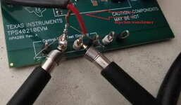
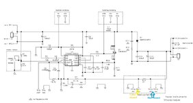
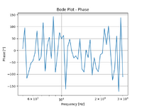
Is it possible to measure the Bode characteristic of the converter using a generator and an oscilloscope? I want to determine the stability reserve of the phase and amplitude. I have a transformer injecting the DHO814 oscilloscope, an FY6900 generator, and I wrote a code in python that injects voltage into the feedback loop on a 51ohm resistor.
I have the impression that my data reading from the oscilloscope is too slow in relation to the regulation. It seems to me that if I read every 100ms, the converter will stabilize by then? Can it be done on the equipment I have?

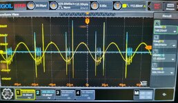
Does the oscilloscope have to be set to the AC range? Because that's what I did

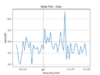
This is how I determine the gain, I don't know if it's right?

amplitude_ratio = (np.max(vout)) / (np.max(vin))
gain_db.append(20 * np.log10(amplitude_ratio))


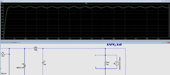
Yellow input waveform and blue output waveform
 

Attachments

  • 1 (1).jpg
    1 (1).jpg
    565.1 KB · Views: 52
  • 1 (2).jpg
    1 (2).jpg
    330.6 KB · Views: 51
  • schematic.JPG
    schematic.JPG
    132.2 KB · Views: 57
  • amplitude.png
    amplitude.png
    33.5 KB · Views: 46
  • phase.png
    phase.png
    42.8 KB · Views: 39
  • TPS.JPG
    TPS.JPG
    65.1 KB · Views: 48
what you can do is use a sig gen ( isolated if necessary ) to inject a sine wave perturbation into the control loop - i.e. the just after the volt ref or demand spot - insert resistor ( say 100 ohm ) if necessary to isolate the Vref - and then look at the output of the converter on AC coupled.

look at the now modified Vref input with the other scope channel

at low freqs the gain can be easily seen ( keep the sig gen amplitude down until you get the feel for it ) - and the phase lag will be minimal

you can write down ( or track and store on a fancy scope ) the gain and phase delay at 100, 200, 500, 700, 1kHz and so on to 10 - 50kHz or so

and then plot. This gives you the plant ( i.e. power converter only, including modulator ) gain and phase.

Fitting an 100 ohm ( say ) injection resistor after the Vref / demand signal - you can look at both sides with your scope and get the full loop gain/phase

but beware injecting noise with your probes - solder a 22k resistor to each point to stop this - p.s. you need a decent scope with good averaging

The sig gen goes across the 100 ohm, you will likely need an isolating injection transformer with near flat characteristics from 10Hz to 100kHz.

You will need less signal at lower freqs, and a little bit more at higher freqs . . .
 
Looks a bit noisy.. The limitation of Bode plots is that it is limited to small or large signal but does not reflect the dynamic range of step currents. Since phase margin and overshoot are reasonably well correlated for 2nd order systems, I would inject active step pulses such as 50~100% , 10~90%,, 0 ~100% using BJTs on a suitable heatsink like an old CPU one.


Capture the voltage errors for various step loads to determine the capabilities and weakest pattern.

I just pulled a random discrete Buck regulator and added an active load with variable amplitude , DC offset and f from 100 Hz to 15 kHz square wave load currents 3.33V up to 100W. https://tinyurl.com/237d5tt6
 
what you can do is use a sig gen ( isolated if necessary ) to inject a sine wave perturbation into the control loop - i.e. into just after the volt ref or demand spot - insert resistor ( say 100 ohm ) if necessary, to isolate the Vref from the sig gen - and then look at the output of the converter on AC coupled.

look at the now modified Vref input with the other scope channel,

at low freqs the gain can be easily seen ( keep the sig gen amplitude down until you get the feel for it ) - and the phase lag will be minimal,

you can write down ( or track and store on a fancy scope ) the gain and phase delay at 10, 50, 100, 200, 500, 700, 1kHz and so on to 10 - 50kHz or so

and then plot. This gives you the plant ( i.e. power converter only, including modulator ) gain and phase.

Fitting an 100 ohm ( say ) injection resistor in the feedback loop, usually after the last error amp, or at the end of the Volt divider as it goes into the Vea - you can look at both sides with your scope and get the full loop gain/phase,

beware injecting noise with your probes - solder a 22k resistor to each point, to go to your probe(s) to stop this - p.s. you need a decent scope with good averaging capabilities.

The sig gen goes across the 100 ohm, you will likely need an isolating injection transformer with near flat characteristics from 10Hz to 100kHz. ( or a couple of large resistors either side back to the sig gen - say 150k each - the sig gen then needs higher o/p capability - 10Vrms gives 3.33mV across the 100 ohm ).

You will need less signal at lower freqs, and a little bit more at higher freqs . . .

happy plotting
 
I did the response to the impulse jump with a transistor, I know this method, but I would like to approach it more professionally. I have an injection transformer, I designed it myself and I measured its bandwidth on VNA, it is not a problem. My problem is, it seems to me, too slow reading from the oscilloscope because I do it after SCPI. I set the generator to 100ms reading, I set the generator to 100ms reading and calculations, but it is probably too slow, the loop has long been after the response to my disturbance, is that right?
 
I don't understand what you mean with "too slow". Loop gain measurement with injected signal should be done in steady state. One problem is selection of injected signal level, it must not exceed linear range of the modulator. Other problem is suitable filtering of response signal out of pwm noise, your results suggest that you are failing at this point. There are commercial instruments like Ridley's AP300 performing similar analysis, in so far there's no doubt that it can work.
 
slow I mean that I am limited in my opinion by communication via scpi commands over USB. Because I output a signal of e.g. 1 kHz then wait 100 ms - that is the delay I have set, but it is probably not a problem (that is what I think now) because when I read with an oscilloscope the disturbing signal is still output and then the oscilloscope reading takes place and I calculate 20 log from the output signal amplitude to the input signal amplitude.

Unless I have something else wrong? In the pictures you can see the oscilloscope connected for the input signal and the second probe from the output signal


One problem is selection of injected signal level, it must not exceed linear range of the modulator.

How to check it and where? The chip I have is TPS40210EVM
ther problem is suitable filtering of response signal out of pwm noise, your results suggest that you are failing at this point.
So how do I get rid of the noise? When I turn on the converter, I can see this kind of noise. I powered the converter with a 9V battery, and the output is 24V. And should the oscilloscope be set to the AC range for both channels? I measure the injected signal with one probe and the output signal with the other.
is it because of this noise and bad amplitude that they do not work properly?
And can it be calculated like this, that the value of the input amplitude to the output amplitude?
 
unless you can average readings to remove the noise - and calc the phase lag between the two signals ( and the magnitude difference for gain ) you may as well give up - noise is the biggest bugbear when trying to do loop gains - hence things are normally run at the highest perturbation levels before it all gets too much for the controller electronics. You could also quiet down the converter with snubbers too.
 
A useable loop gain analyzer performs synchronous demodulation of measured signal with generated signal as reference. This way noise and out of band spurs, e.g. pwm carrier are suppressed. A prerequisite for meaningful results are stable control loop and absence of subharmonics in the frequency range of interest.
 
Here is an LTspice sim showing what you have to do.
Keep your eye on the COMP pin...your loop injection shouldnt be so big that the COMP pin voltage goes to its rails.

The injection point should see high Z looking one way, and low Z looking the other way.
Unless its a type of injection method that doesnt require this of course (eg the way its recomended to do it on those powerint flyback chips)
 

Attachments

  • buck 12v to 5v at 1A_loopmeas.zip
    1.8 KB · Views: 14
  • Loop meas.png
    Loop meas.png
    62.2 KB · Views: 23
  • __Loop Gain Measurement.zip
    334 KB · Views: 15
The injection point should see high Z looking one way, and low Z looking the other way.
That's actually not the case in your example. You better choose top of R4 as injection point.

Loop gain is defined the wrong way in your schematic. It's A/B, voltage at switcher output/voltage at feedback input.

Measurement setup in post #1 is o.k., problem is analyzer performance.
 
Thanks, yes thats right, my apologies it was a slack copyAndPaste from a different thing.
The attached shows the correction. (LTspice and PNG)
 

Attachments

  • Loop Meas _1.png
    Loop Meas _1.png
    54.8 KB · Views: 17
  • buck 12v to 5v at 1A_loopmeas_1.zip
    1.7 KB · Views: 14
Last edited:
Thank you for the simulation files.
To do such simulations for a given converter I would have to have its integrated circuit model in order to select the feedback elements?

I always checked the response to a single step and based on that I determined the stability and it is a good method, but I would like to try something new.

So GAIN according to the diagram in LtSpice is 20log(A/B). Can I take the amplitude - the maximum value of signal A and the maximum value of signal B - to determine GAIN?

Why do converters have a large GAIN at the beginning of low frequencies? And what does it mean that it is good bad and why?
If the GAIN is high at the beginning, does it mean that when the voltage drops, the converter will be able to respond quickly and with high gain without overshooting?

The diagram says "When A pkpk = Bpkpk then you are at crossover freq" it means that GAIN = 0dB and you can determine the phase margin, but what else does this information give me. How many dB per decade should the GAIN fall and why does it decrease with increasing frequency?


why on the second oscilloscope probe I see 0V on the low impedance side and on the high side where the feedback is I see a sine signal?

Noise ingress on the injection point into high impedance unbalanced inputs can be hampered by common mode noise. Thus it is imperative to respect that and use very low impedance twisted pair such as magnet wire or coax.


I made an injection transformer from a twisted pair of internet cable and the core I took from a common-mode filter, exactly two cores and a winding wound on it.But the output injection wires at the resistor soldering point were not twisted so that needs to be fixed
 
Last edited:
why on the second oscilloscope probe I see 0V on the low impedance side and on the high side where the feedback is I see a sine signal?
On the lab bench you see this?.....well it sounds like you are either using too small an injection signal...or perhaps you are injecting at a frequency well above the crossover frequency

So GAIN according to the diagram in LtSpice is 20log(A/B). Can I take the amplitude - the maximum value of signal A and the maximum value of signal B - to determine GAIN?
By amplitude you mean "peak" or "pk2pk"?
...But yes you can take either..
 
I will do some more tests and see what comes out.

I understand Amplitude as in the picture below, but I know that there are different interpretations of it. And as I indicated, I take the maximum value of the amplitude of point A and divide it by the maximum value of point B
 

Attachments

  • 435345345345.JPG
    435345345345.JPG
    23.3 KB · Views: 9
Why do converters have a large GAIN at the beginning of low frequencies?
Because the error amplifier is an opamp integrator, which has capacitive connection in the feedback path...and capacitor is super high Z at low frequency, and hence the error amplifier has super high gain at low frequency.

High gain at low freq means accurate vout at low freq......to know this it helps to know about ideal opamp theory, and how they have super high gain in ideal world, and if you go through derivation of the Vout/Vin = -Rf/Rin for an inverting amp then you will realise why a high gain gives you accurate vout.

..Remember the ideal GND?....remember that the + and - inputs of an opamp with neg feedback are the same...but not exactly the same....if gain is low then they are further apart.....etc etc..

f the GAIN is high at the beginning, does it mean that when the voltage drops, the converter will be able to respond quickly and with high gain without overshooting?
...it may still overshoot...it depends

To do such simulations for a given converter I would have to have its integrated circuit model in order to select the feedback elements?
Well yes you need to know if it is voltage mode or currnt mode...and you need to know the current sense threshold voltage....and if the error signal is divided down b4 going into the pwm comparator........ then you need to know that so that you can incorporate it into bode plot calcs.
 
Sure, I understand now, the entire converter can be treated as a small box, which is an operational amplifier + also LC filters in the converter at the output
..Remember the ideal GND?....remember that the + and - inputs of an opamp with neg feedback are the same...but not exactly the same....if gain is low then they are further apart.....etc etc..

In the sense that the system can become a generator despite the hidden feedback?

you need to know the current sense threshold voltage

Could you show more information on this topic and how to choose the pk-pk value of the injection signal depending on the IC documentation? What to look for?
I found some information like that, I also added the scalak documentation

I found the open loop error amplifier gain and it is very high, which also explains why at low frequency the gain is high


----------------------

Regarding simulation
When there is 1 kHz in the simulation, it can be seen that the system is unstable, when I made a different frequency, it was visible that it is stable, so this shows that it probably has a small phase margin?
 

Attachments

  • Amplifier.JPG
    Amplifier.JPG
    45.9 KB · Views: 9
  • Overcurrent.JPG
    Overcurrent.JPG
    63.8 KB · Views: 10
  • SYM.JPG
    SYM.JPG
    162.6 KB · Views: 11
  • TPS40210EVM.pdf
    1.8 MB · Views: 11


Write your reply...

LaTeX Commands Quick-Menu:

Similar threads

Part and Inventory Search

Welcome to EDABoard.com

Sponsor

Back
Top