Continue to Site

Welcome to EDAboard.com

Welcome to our site! EDAboard.com is an international Electronics Discussion Forum focused on EDA software, circuits, schematics, books, theory, papers, asic, pld, 8051, DSP, Network, RF, Analog Design, PCB, Service Manuals... and a whole lot more! To participate you need to register. Registration is free. Click here to register now.

Balanced OTA-C cascode IC design

Status
Not open for further replies.
Oh, I misunderstood what you meant, Yes I have actually connected both circles together with the output of the non differential ota, the problem that I mentioned in my last comment was when I connected the differential ota with my non differential ota, or to be precis replacing the vcmfb node at the differential with vcmfb_amp, the result was most transistors in the differential ota went to triode region and the output voltage at vout+ and vout- was around 20 mV rather than 600mV, so just to make sure , there is nothing wrong in my circuit connections or any concept that I implemented in correctly? maybe I need to change transistors parameters only? I thought that I wouldnt need to change parameters since the non ideal circuit should behave close to the ideal one, not identical but should have atleast close results. a quick question also, my ideal vcvs has a gain of 100 however the non differential ota has a gain of only 72, but that shouldnt be a great problem right?
 
Last edited:

Yeah, 72 should be enough. Maybe, I don't know. Could you post some pictures about the annotated schematics?
 
Yeah, 72 should be enough. Maybe, I don't know. Could you post some pictures about the annotated schematics?

Well I managed to get a 597mV at the vout+ and vout- using the non ideal circuit, do I need to get an exact value of 600mV or 597 is fine ? the second question would be the following, attached are two screenshots of the node voltages using the ideal circuit-vcvs- and two screenshots of the node voltages using the non ideal circuit - non differential ota- and the gain in the non differential ota before connecting it to the differential ota and after connecting ,I thought that gain should be similar in both as it is the same circuit obviously but the gain changed vastly, before connecting it was a proper gain of 72.5 as attached, after connecting it is this weird plot, is that normal?
 

Attachments

  • Ideal1.PNG
    Ideal1.PNG
    36.7 KB · Views: 95
  • Ideal_2.PNG
    Ideal_2.PNG
    21.4 KB · Views: 89
  • Non ideal.PNG
    Non ideal.PNG
    44.6 KB · Views: 94
  • Non_Ideal2.PNG
    Non_Ideal2.PNG
    24.2 KB · Views: 94
  • Gain.PNG
    Gain.PNG
    60 KB · Views: 97
  • CMFB_Gain.PNG
    CMFB_Gain.PNG
    63.6 KB · Views: 86

Fine. And you can delete the 10MOhm resistor, It has no function. The gain changed because the diff. amp's 2nd stage increased the gain of the CMFB loop. It is normal.
 
Fine. And you can delete the 10MOhm resistor, It has no function. The gain changed because the diff. amp's 2nd stage increased the gain of the CMFB loop. It is normal.

I figured I might check for the circuit stability and I did and unfortunately after I thought I was done with this circuit ,the circuit showed to be unstable as you can see in the loop gain screenshot, do you have any idea what should I do to stabilize the circuit ?
 

Attachments

  • Gain.PNG
    Gain.PNG
    62.1 KB · Views: 87
  • Loop Gain.PNG
    Loop Gain.PNG
    88.3 KB · Views: 87
  • Analysis.PNG
    Analysis.PNG
    17.6 KB · Views: 98

Sorry, but could you plot a decent Bode diagramm? Where the gain really reaches the 0dB and where anybody can see that how much is the maximum loop gain and where is the dominant pole and the others.
Sweep from 1Hz to 1GHz the frequency, use logaritmic sweep, at least 30 points per decade.
 

Sorry for the late reply I was away for a couple of days, well the problem was actually straight forward I was just focusing on biasing the circuit and forgot to add the capacitance of my gm-c filter which is kind of ironic, once I added the capacitance at the differential outputs the circuit was stable, however the problem now is my gm value bandwidth is not good enough, I am using a 5p F at the differential outputs as attached,I am operating at an IF 1-3 MHz channel, as you can see the marker at 1 MHz is almost at the transition region of the gm value which lets my gm value change somehow at the start of my channel from the value at the end of my channel if i increase the capacitance value to around 10p at each differential output the bandwidth increases and is somehow good however I was told that since I have 9 OTAS in my circuit I can't use about 20p F in each OTA as this would make me some trouble when I am in the layout designing phase, I have no idea what to do from here to get a better compromise between bandwidth and making layout easier?
 

Attachments

  • 1p.PNG
    1p.PNG
    63.6 KB · Views: 93
  • 5p.PNG
    5p.PNG
    56.9 KB · Views: 88
  • 10p.PNG
    10p.PNG
    63 KB · Views: 98
  • OTA.PNG
    OTA.PNG
    32.9 KB · Views: 92
Last edited:

You cannot measure in AC with small capacitances the Gm. At lower frequencies the reactance of the capacitor is higher and the current through it is lower. It is natural the Gm drops because you calculate it wrongly. Don't worry about this, your Gm actually is the same as at higher frequencies, you can use the smaller capacitors.
 

So it is just a miscalculation and even if I use the 1p capacitors the gm value should be Okay at my low IF right?

- - - Updated - - -

and if you do not mind , how can i calculate the gm value accurately then? because as far as the simulator can see if I cascade my 9 OTAs and each of them has a varying gm value between 1 MHz and 3 MHz won't the response be not as designed in my IF 1-3 MHz channel due to this varying value ?
 

I think we have discussed it already. Put a large capacitor to the output, measure the current through that.
Gm=magnitude(I_C)/magnitude(Vin)
 

I understand, but what I meant as far as the simulator is concerned while using the 5p capacitor the gm value is not constant between 1-3 MHz, if i use the small capacitor with the variable gm value - according to the simulator- wont the simulator plot a weird output aftet cascading all the stages together rather than my filter due to the varying gm value ?
 

No, Gm is constant at lower frequencies too, whatever how much is your load capacitor, it is not changing between 1-3MHz, just you don't know why not and you don't know what are you calculating.
With the small capacitor the Gm seems lower but it is not lower!!! Please understand if you want to measure the Gm with small capacitor then you will get false result at lower frequencies!
And please learn more from books, you don't know what you are doing.
 

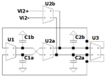
well you misunderstood my question, but yes I understand what you are saying and I know you are absolutely right, however I have a quick question in regards to the installation of the circuit, as you already know my circuit had single ended output ideally, but now I have a differential output circuit, so I am just having some trouble finding how to connect the differential circuit, as far as I understand it should be as I drawn in the attached picture, would that be correct? attached is a figure of the single ended circuit and my differential circuit
 

Attachments

  • Thomas.PNG
    Thomas.PNG
    46.6 KB · Views: 100
  • Tow Thomas.jpg
    Tow Thomas.jpg
    467.1 KB · Views: 84

Obviously Vi is shorting C1 in your differential circuit version.

- - - Updated - - -

A series connection of C1 and Vi is at least a theoretical option to perform the signal summing in the differential circuit.
 

Obviously Vi is shorting C1 in your differential circuit version.

- - - Updated - - -

A series connection of C1 and Vi is at least a theoretical option to perform the signal summing in the differential circuit.

but other than the C1 and Vi problem the rest of the circuit should be correct right ?

- - - Updated - - -

Obviously Vi is shorting C1 in your differential circuit version.

- - - Updated - - -

A series connection of C1 and Vi is at least a theoretical option to perform the signal summing in the differential circuit.

and what do you mean by a theoritical option? shouldn't this connection + your tip work fine ?

- - - Updated - - -

After thinking about it, shouldn't the series connection block the dc input part of the input sin wave voltage source? It won't work that way I guess
 

The current configuration is a band pass, in this case Vi DC level shouldn't matter. Alternatively you can use two differential OTAs in parallel feeding C2, one for Vi and one for the feedback loop.
 

I understand the current configuration is bandpass but wont thr lack of the dc voltage affect the biasing of the transistors in the ota? For the alternative i thought of that option but i would have 4 outputs then from the second ota,how would I reduce them again to 2 outputs for the third ota ?
 

It's expected that the negative DC feedback achieves correct bias independent of the input voltage (as long Vi doesn't the accepted voltage range).

OTAs are controlled current sources, the outputs can be parallel connected without affecting the other signal path.
 

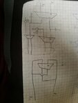
What do you mean by the outputs can be parallel connected while not affecting the other signal path? Just to make sure we are talking about the same thing, by using parallel otas we are talking about having 2 parallel otas identical to the original tow thomas right? Each ota has one differential output from the previous ota with a capacitor and the other input would be the input signalIMG_20180417_171432_1.jpg
 

Status
Not open for further replies.

Part and Inventory Search

Welcome to EDABoard.com

Sponsor

Back
Top