LMK__
Newbie

Hi,
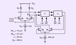
I have to design a DFE circuit for the LPDDR5 receiver. I have created a simple 1-tap DFE circuit that is shown in Razavi's article (link: https://ieeexplore.ieee.org/document/9694443 , figure 9), and its behavior with regard to its input seems reasonable. However, I do not know how to proceed further.
First of all, the tap coefficient should be adjusted according to the channel output, and for this, one needs to simulate the channel and see how it distorts the digital input. I want to know, how can one simulate a channel in using "n6port" and "mtline" blocks in Cadence Virtuoso? I have S-parameter file for the n6port, but I don't know how to set the other parameters to have a realistic channel output.
Secondly, is there a systematic way to determine the tap coefficient, or is it just trial-and-error?
Thirdly, I cannot decide what to keep in mind for sizing the circuit. As far as I know, the ratios of transistor widths will depend on the tap coefficient, but what about exact numbers? Which parameters of the circuit should be deciding factors for sizing? And how can I decide what values those parameters should have?
And lastly, I cannot really figure out what a normal LPDDR receiver without DFE looks like and in which part the DFE should fit in. I have read many papers but I could not really get the background info on how a basic LPDDR receiver should be designed, since most papers just suggest an overall view architecture and show the results without going into specifics. Could someone suggest good sources that explain DRAM receiver circuits and possibly analog DFE circuits in more depth?
Those questions could seem silly since I am new to this field, and would appreciate any guidance.
Thanks in advance

