Continue to Site

Welcome to EDAboard.com

Welcome to our site! EDAboard.com is an international Electronics Discussion Forum focused on EDA software, circuits, schematics, books, theory, papers, asic, pld, 8051, DSP, Network, RF, Analog Design, PCB, Service Manuals... and a whole lot more! To participate you need to register. Registration is free. Click here to register now.

a high side load switch made from n channel and p channel mosfet working principle

oppel

Newbie level 6
Joined
Dec 13, 2023
Messages
12
Helped
0
Reputation
0
Reaction score
0
Trophy points
1
Activity points
75
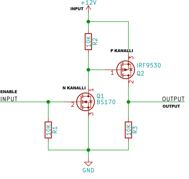
Hello, I did research on the internet to understand the working principle of the circuit you see in the image, but I could not find an article that explains exactly how the N-channel and P-channel MOSFETs used here work according to their transmission cut-off states.

I would appreciate it if you could give detailed information about the working principle of this circuit.
Ekran Alıntısı.PNG
 
The N MOSFET L

1714385212374.png


As you can see when the Vgs goes positive the drain current increases from
~ 0 mA to some value based on its geometry. That in turn generates the Vgs
for the P MOSFET via R2 :

1714385578346.png


And so its drain current increases with increasing Vgs and that causes the output at R3 to increase in V.

Keep in mind the souce of the N MOSFET is grounded whereas that of the P MOSFET is tied to + supply.

So Vgs = V gate to source, and is typically operated + for N MOSFET, and negative for P MOSFET.

Also the above are for enhancement mode MOSFETs, look up depletion mode to see how increasing
Vgs reduces Idrain.


Regards, Dana.
 
The N MOSFET L

View attachment 190443

As you can see when the Vgs goes positive the drain current increases from
~ 0 mA to some value based on its geometry. That in turn generates the Vgs
for the P MOSFET via R2 :

View attachment 190445

And so its drain current increases with increasing Vgs and that causes the output at R3 to increase in V.

Keep in mind the souce of the N MOSFET is grounded whereas that of the P MOSFET is tied to + supply.

So Vgs = V gate to source, and is typically operated + for N MOSFET, and negative for P MOSFET.

Also the above are for enhancement mode MOSFETs, look up depletion mode to see how increasing
Vgs reduces Idrain.


Regards, Dana.

Thank you for explaining the operation of N-channel mosfet. So, what is the working logic of the circuit with active?
 
Rs can be thought of several ways :

1) Convert current to a V
2) Form a divider with other Rs to create an attenuator
3) Limit current in a circuit
--- Updated ---

This might help :

1714387612343.png
 
Last edited:
Essentially circuit switches power on and off to output load, which is
grounded one side, R3 in your original schematic.

R1 in your original schematic keeps both MOSFETS off if no input connection
is applied to circuit. A mosfet, being very high Zin at DC, is subject to leakage
currents and stray pickup. So reason to insure if no connection is made, or
if input is driven by a source that is in tristate mode, the output is in a known state.


Regards, Dana.
 
Last edited:
Hi,

you are free to do an internet search: "how do MOSFETs work".

Since everyone who starts with electronics needs to learn it.. there are thousands of hits.

From basic descriptions to more detailed ones. PDFs, internet pages, even videos.... in many languages.

Klaus
 
The arrangement of the two transistors is a convenient method by which a weak signal is able to control a P-device (Q2). And R2 is necessary to provide Q2 bias with a reference to supply voltage. This allows the P-device to be biased with a definite voltage which has some shutting-off effect, in counter to Q1 providing turn-on bias from 0V gnd.
 

LaTeX Commands Quick-Menu:

Part and Inventory Search

Welcome to EDABoard.com

Sponsor

Back
Top