Continue to Site

Welcome to EDAboard.com

Welcome to our site! EDAboard.com is an international Electronics Discussion Forum focused on EDA software, circuits, schematics, books, theory, papers, asic, pld, 8051, DSP, Network, RF, Analog Design, PCB, Service Manuals... and a whole lot more! To participate you need to register. Registration is free. Click here to register now.

500VA sine wave inverter , problem in HBridge and filter designing

Status
Not open for further replies.
ok you can try by adding resistor of some mili ohms to the drain of mosfet & amplify it by any opamp. or you can use a current sensing transformer at the o/p 230v of inverter. i will search a detailed schematic
 
pradeep,,if i use a TVS diode at each mosfet ,will it be able to protect my mosfet from transient,?
because i have tried everything , like applying damper(220v 100w bulb in series with C) in my lc filter, changing gate resistor to 50ohm, increasing bootstrap capacitor etc,,
i think the problem is due to high voltage spike from back emf of inductor, as when my switch comes in off state, the current start decreasing rapidly which results in high voltage spike dv/dt ,
so my mosfets will be in stress,which might be result in breakdown of mosfets . i am not sure whether i am right or wrong..its just what i am thinking.
i havn't tried TVS diode ,,can u suggest me any TVS diode which will solve my purpose, also is it necessary to use dc bus capacitor near the hbridge circuit , beacause my dc bus capacitor is not near my h bridge circuit ,it is on another board.
 

in my opinion its not a back emf. why cant you try a 2.2mfd/440vac fan capacitor instead of lc filter. and see the waveform.

assume that if their is a short circuit in o/p side i mean o/p 230volt is shorted then how safe is your mosfet
 

is it necessary to use dc bus capacitor near the hbridge circuit , beacause my dc bus capacitor is not near my h bridge circuit ,it is on another board.
It's absolutely required. I think it has been mentioned by several contributors in your previous thread.

Is the previously shown stripboard photo still valid? We never saw it's bottom side. https://obrazki.elektroda.pl/3396086000_1372181551.jpg

A short comment about the current limiting point. It's basically a good idea to have some kind of overload protection, e.g. to handle load shorts. But in the present case we are talking about "spontaneous" failure in normal operation. There's no indication for an overload and the overcurrent sense possibly won't react before the transistors are blown.
 

i am using 0.22uf capacitor and 5mh inductor,
i have used ETD39 core (1mm gapped) for making inductor,
inverter rating is 220v 400VA approx. 50hz,,, carrier frequency is 16khz ,
is this not a correct value?

From running a simple simulation, it appears as though these values work okay at 16 kHz. The capacitor charge drops only slightly during idle gaps. (This is only a tentative finding. It does not tell everything about your waveform. That is changing constantly.)

You say a resistive load alone is not a problem. Yet you get problems after installing the LC low-pass filter.

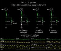
Because it sounded as though the LC filter is draining excessive current to ground, I followed up with further simulations.

The left-hand circuit shows your stated values. The other three are the same except a component is altered by fifty percent.

Results show that current will rise if either the coil value or the frequency is reduced. However even when those are reduced fifty percent, current does not become so great that it has to barbeque your mosfets.

Again this can only be a tentative theoretical result.

 
i am using 0.22uf capacitor and 5mh inductor,
i have used ETD39 core (1mm gapped) for making inductor,
inverter rating is 220v 400VA approx. 50hz,,, carrier frequency is 16khz ,
is this not a correct value?

By using this series LC method the waveform and circuit characteristics changes with the connected load so it was very complicated to describe for every load so it was no commonly used and the best method is pwm controlled method for a inductive load you don need any filtering on it.....
 

By using this series LC method the waveform and circuit characteristics changes with the connected load so it was very complicated to describe for every load so it was no commonly used and the best method is pwm controlled method for a inductive load you don need any filtering on it.....
The filter effect should be analyzed in two regards:
- effects at mains frequency
- effects at switching frequency

At the mains frequency, you have a small inductive (Xk=1.3 % with the present dimenioning) voltage drop which can be neglected. Up to 5% Xk (Xk=XL*In/Vn) would be acceptable if necessary. This gives room for increasing the inductance if a stronger filtering is intended. But it would also involve an unwanted large inductor size.

At the switching frequency, the filter impedance is inductive, causing about 0.3 A reactive current. This should be acceptable for a well designed inverter related to the rated output current. Similar or even higher reactive current can be consumed by inductive loads, e.g. motors. We can expect that an inverter failing with a low-pass filter will show problems with other kinds of reactive loads too.
 
At the switching frequency, the filter impedance is inductive, causing about 0.3 A reactive current. This should be acceptable for a well designed inverter related to the rated output current. Similar or even higher reactive current can be consumed by inductive loads, e.g. motors. We can expect that an inverter failing with a low-pass filter will show problems with other kinds of reactive loads too.

what is the triggering scheme and filtering used in three phase pwm inverter, the problem is every phase is available in all 360 degree and if we set the maximum duty cycle is 33 percent what will be the effect in transformer....?
 

today i have simulated my LC filter unit step response on MATLAB. below are the attachments

CASE 1 -unit step response when L=5mh, C=0.22uf
0.png
in above image it can be easily seen that output voltage has a gain of approx 25, so if my SPWM is 311V the output might be 311*25=7775v, so i this can be the resaon for failure of mosfets.

CASE 2- 488ohm resistance is used in series with capacitor to damp the oscillations, L=5mh , C=0.22uf, R=488 ohm
488.png
in above image ,oscillations are damped ,but still my circuit failed. i have used a 220v 100w bulb as a damping resistor in series with capacitor.

CASE 3- 75ohm resistance is used in series with capacitor, L=5mh, C=0.22uf , R=75 ohm
75.png
in the above image the gain is nearly 1. i havn't tried this circuit practically, should i try this resistance in my real circuit.??
also suggest some TVS diode that can be put across each mosfet.so that it can protect the mosfet from spikes.?
 

in above image it can be easily seen that output voltage has a gain of approx 25, so if my SPWM is 311V the output might be 311*25=7775v, so i this can be the resaon for failure of mosfets.

what do you mean gain 25, is any passive filter will give you any gain????
 

Transients of 7,775 V...

Are the same as high-voltage spikes.
Such as are caused from switching off a coil while it is carrying current. (Although I cannot say what coil is producing these spikes.)

Have you tried omitting the coil? To see if the capacitor could be sufficient to smooth your PWM? (This was suggested in post #25.)
 
Besides the point that the filter simulation doesn't describe a retroaction to the input, I really wonder how you get more than 2 Vpp output voltage from a 1 V input step. That's just impossible, as simple conservation of energy problem.

Feeding a periodical signal near the resonance frequency to the unloaded and undampened filter can in fact generate a high output voltage and possibly exceed the component ratings. But you won't do that.
 

BradtheRad said:
Have you tried omitting the coil? To see if the capacitor could be sufficient to smooth your PWM?
capacitor will draw a huge reactive current ,which might be greater than rated inverter output current,so i think it's not a good choice.

as i earlier mentioned that my h bridge circuit is working fine ,when i am not using any filter, i have checked it by connecting 220v 100watt bulb to h bridge output.
as i connect LC filter ,my mosfets gets damaged, so the possible reason may be , either shoot through by turning on both the mosfet of same leg, as i have provided sufficient deadtime, so is it possible that any back emf from LC filter is responsible for turning on my mosfet which is intended to be in off state,?
 

I think the most probable reasons for damaging the MOSFET will be higher current or higher Off time voltage.... By putting parallel diode it was impossible apply any reverse voltage, so the problem is higher current....

May be the capacitance value you choose for filter is high enough to damage the current, so next time just use a capacitor series to your load and select the capacitor as enough to have a sine wave so it wont damage the MOSFET and wont make any unwanted current path from DC source....

what i am trying to say is try a series LC filter with series to load so there is no any chance for damaging the device...

- - - Updated - - -

I think you are trying this


but instead try this......

**broken link removed**
 

so is it possible that any back emf from LC filter is responsible for turning on my mosfet which is intended to be in off state,?

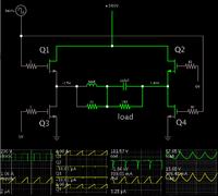
I am trying a different simulation. It shows the coil can generate high-voltage spikes at switch-Off.


The H-bridge has two mosfets sending 16 kHz pulses of one polarity through the load and LC butterworth filter. (The other two mosfets remain off for 1/50 sec.)

Between 16kHz pulses, both switching devices (mosfets) become high impedance. (Notice this is different from my simulation in post #27 where the input alternated between supply V and ground.)

The scope traces reveal a spike across the coil when it is switched off. Upwards of 2 kV.

This circuit may not be the same as yours.
 

It shows the coil can generate high-voltage spikes at switch-Off.
The error in simulation setup: It apparently uses MOSFETs without backward (substrate) diodes. They don't exist as technical devices.

In a real inverter, the diodes clamp the inductor flyback voltage to the power supply.
 

Status
Not open for further replies.

Similar threads

Part and Inventory Search

Welcome to EDABoard.com

Sponsor

Back
Top