ferdem
Full Member level 2

Hi! I'm working on a delayline frequency discriminator setup to measure phase noise. I realized that my measurement results stay the same below 100 KHz regardless of how pure the input signal is (it is dominated by some other noise). I'm able to see expected results above 100 KHz.
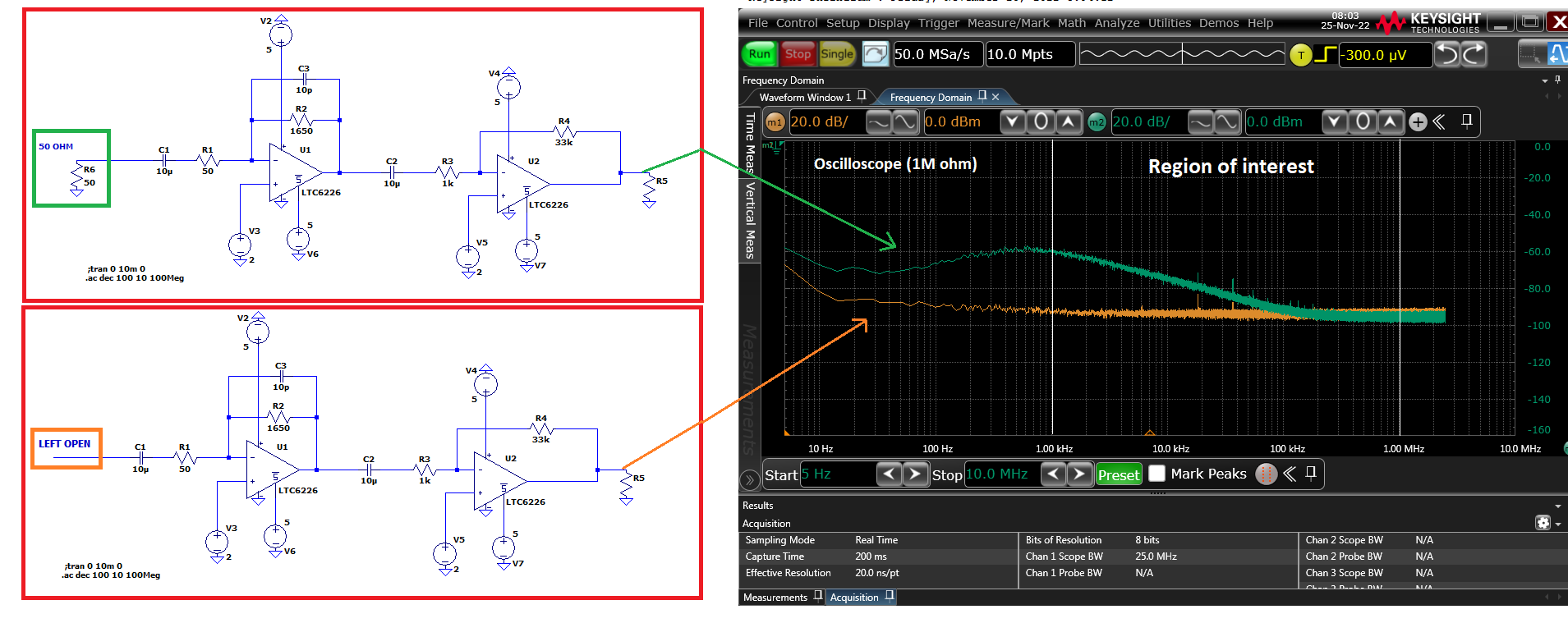
The problematic part is my baseband amplifier consisting of two OPAMP stages (Total: 960 V/V, ~60 dB), see the below schematics.
I examined the baseband amplifier separately and conducted following experiment:
When I left open the input, I observe a certain noise level at the output. When I connect a 50 ohm to the input, the noise power increases below 100 KHz (depicted in the image). The phenomenon I observe here should be the reason of why I m not able to measure phase noise below 100 KHz offset.
What could be the reason of this noise? Why does it increase unevenly? In LT6226's datasheet, input noise voltage spectral density looks flat between 1 KHz and 1 MHz.
Is there a way to diminish this noise?
I'm using a benchtop power supply and I believe that sufficient filtering (ferrites and capacitors) on supply and reference IC voltages is provided.
Any comments will be welcome.
Thanks.

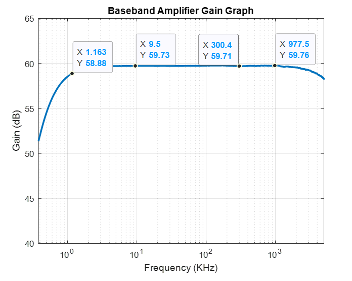
Here is the gain of the baseband amplifier:

The problematic part is my baseband amplifier consisting of two OPAMP stages (Total: 960 V/V, ~60 dB), see the below schematics.
I examined the baseband amplifier separately and conducted following experiment:
When I left open the input, I observe a certain noise level at the output. When I connect a 50 ohm to the input, the noise power increases below 100 KHz (depicted in the image). The phenomenon I observe here should be the reason of why I m not able to measure phase noise below 100 KHz offset.
What could be the reason of this noise? Why does it increase unevenly? In LT6226's datasheet, input noise voltage spectral density looks flat between 1 KHz and 1 MHz.
Is there a way to diminish this noise?
I'm using a benchtop power supply and I believe that sufficient filtering (ferrites and capacitors) on supply and reference IC voltages is provided.
Any comments will be welcome.
Thanks.
Here is the gain of the baseband amplifier:


