eengr
Member level 4

Hi All
I am current working on a circuit design which involves interfacing an O2 gas sensor
I tried to reverse engineer the development board from manufacturer (They don’t supply the schematics)
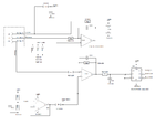
And I believe the circuit that has been used looks something like as shown in the picture below:

It is a three terminal Electrochemical type sensor which as three electrodes as:
Counter Electrode
Reference Electrode
Working Electrode
(As shown in schematic above)
IC2a,2b&2c is in same package Dual Opamp AD8629 from Analog devices (Datasheet @ https://www.analog.com/media/en/technical-documentation/data-sheets/ad8628_8629_8630.pdf )
I believe that IC2b is used in Control feedback like Potentiostatic configuration in order to maintain the potential of Reference Electrode similar as Working Electrode
IC2c is used to convert the signal output (current) from the sensor to the Voltage output (Isense X R28). This signal is then fed to ADC MCP3550 (22bits) from Microchip (Datasheet @
https://ww1.microchip.com/downloads/en/DeviceDoc/20001950F.pdf )
3.85VDC is coming out of a voltage regulator (not shown on schematic). The input to that regulator is from 5VDC
I am current working on a circuit design which involves interfacing an O2 gas sensor
I tried to reverse engineer the development board from manufacturer (They don’t supply the schematics)
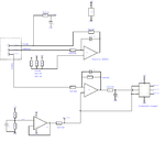
And I believe the circuit that has been used looks something like as shown in the picture below:

It is a three terminal Electrochemical type sensor which as three electrodes as:
Counter Electrode
Reference Electrode
Working Electrode
(As shown in schematic above)
IC2a,2b&2c is in same package Dual Opamp AD8629 from Analog devices (Datasheet @ https://www.analog.com/media/en/technical-documentation/data-sheets/ad8628_8629_8630.pdf )
I believe that IC2b is used in Control feedback like Potentiostatic configuration in order to maintain the potential of Reference Electrode similar as Working Electrode
IC2c is used to convert the signal output (current) from the sensor to the Voltage output (Isense X R28). This signal is then fed to ADC MCP3550 (22bits) from Microchip (Datasheet @
https://ww1.microchip.com/downloads/en/DeviceDoc/20001950F.pdf )
3.85VDC is coming out of a voltage regulator (not shown on schematic). The input to that regulator is from 5VDC
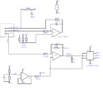
My first question is regarding the reference voltage (VRef in the schematic of apprx 1.923V as measured by DVM)
The way I understand it (and I could be wrong so please correct me). The VRef (1.923V) is applied to non-inverting input of IC2c which will give it a DC offset so we should see the Signal Output from IC2c as (1.923V + (Isense x R28))
This Vref of 1.928 is also applied to ‘VREF’ pin-1 of ADC MC3550 so it sets its Reference voltage to this level
But why does it have ‘VRef (1.923V)’ connected to the Negative Input of (VIN- Pin3) of ADC?
How is this going to work? Would that not cause the ‘Signal of interest’ between VIN+ & VIN- to go higher than the Reference voltage of ADC?
My 2nd question is regarding the summing junction at non-inverting pin of IC2b.
‘VRef’ which is connected to R23
3.85V which is connected to R25
& then the node of R23 & R25 are connected to non-inverting pin of IC2b. What would be the purpose of that configuration?
My 3rd question is regarding the resistors R33 & Cap C14. It looks like that Counter electrode is connected to one of the pins of PIC microcontroller on development board. Any idea why would this connection to PIC be required? Is it some sort of detection?


