Continue to Site

Welcome to EDAboard.com

Welcome to our site! EDAboard.com is an international Electronics Discussion Forum focused on EDA software, circuits, schematics, books, theory, papers, asic, pld, 8051, DSP, Network, RF, Analog Design, PCB, Service Manuals... and a whole lot more! To participate you need to register. Registration is free. Click here to register now.

[SOLVED] What's the difference between stacked and cascode configurations?

Status
Not open for further replies.

Fávero Santos

Junior Member level 1
Joined
Jul 9, 2013
Messages
15
Helped
0
Reputation
0
Reaction score
0
Trophy points
1,281
Activity points
1,440
Hi, all

I saw in an article that the authors differentiate the terms stacked configuration and cascode, even though in my opinion the stacked configuration is basically a cascode configuration.

Could you please help me elucidate this issue?

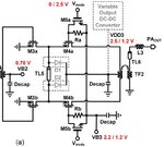
The image available in the following link is a cut of the image present in the paper "A 60 GHz CMOS Dual Mode Power Amplifier With Efficiency Enhancement at Low Output Power" by Lixue Kuang, Baoyong Chi, Haikun Jia, Wen Jia and Zhihua Wang.
fOizzMr.jpg
https://imgur.com/a/U9Ua1B5

Many thanks!
 

Cascode tends to imply a "common base" stage on top of
a common-emitter (or, gate/source for you youngsters)
and a common-base (gate) stage has no activity, just a
static bias of low impedance.

Stacked stages can co-drive the two (or more) FETs,
this can be a useful play when (say) you have a much
higher rated Vgs than you have Vds (or can level shift
each gate suitably).

It looks like there is a modal gate resistor here, that puts
the circuit either into a normal cascode (switch closed,
Vmode is DC bias w/ "Decap" knocking down the HF
impedance) or a "live" RC connected gate. I have seen
some folks use resistor biased gates for both RF switches
(resistor, static/digitla switched) and for active amps where
a properly tuned gate lets the top FETs (M5_) add gate
activity to the amplifier (making the output low, rather
than high impedance at least on one phase of the cycle).

Because it's not always DC-pinned I would not call it a
classical cascode. Modal, cascode in one logic setting,
perhaps.
 
Great explanation dick_freebird.
I would summarise by saying, cascode is a common gate (Vbias cascode and RF gnd) and in stacked the gate is connected to Vbias through R and to gnd via a capacitor so that the RF signal at the drain of the first transistor finds a second RF path to gnd and part of RF signal is fed to the gate of the stacking transistor.
 

In cascode mode your upper transistor gate is AC grounded and it acts as load to increase your output resistance.
In some designs people do not make AC ground at the gate but they connect to a small capacitor which allows swing in gate.
Drawback is you will have less gain since your gate has swing but advantage is gate will swing in phase with drain so you can avoid breakdown.
That is how you can stack 3 transistors for example and gate high Pout while preventing transistor breakdown.
 
Status
Not open for further replies.

Part and Inventory Search

Welcome to EDABoard.com

Sponsor

Back
Top