Continue to Site

Welcome to EDAboard.com

Welcome to our site! EDAboard.com is an international Electronics Discussion Forum focused on EDA software, circuits, schematics, books, theory, papers, asic, pld, 8051, DSP, Network, RF, Analog Design, PCB, Service Manuals... and a whole lot more! To participate you need to register. Registration is free. Click here to register now.

Op Amp malfunction in SallenKey Filter configuration with Gain

Status
Not open for further replies.

fouwad

Full Member level 4
Full Member level 4
Joined
Nov 29, 2009
Messages
199
Helped
19
Reputation
38
Reaction score
17
Trophy points
1,298
Location
Pakistan
Activity points
2,466
Hi, I am designing a Data Acquisition System for RTDs, for which i used this application note for analog part. ww1.microchip.com/downloads/en/appnotes/00687c.pdf

I used ADA4004-2 Op Amps instead of MCP609. The application note used 7.47 Gain V/V while i used 8V/V. Moreover, i added another Gain stage(just simple non inverting Gain) after the Filter+Gain stage. The Gain value for next stage is 2.5-5V/V.
Now the issue is that the Op-Amp used in SallenKey+Gain configuration keeps on malfunctioning after some time or is permanently damaged giving saturated value of +15V or -15V. When i replace this OpAmp, new one starts working fine until it faces the fate of the old one.
I would like to add one more thing that i am multiplexing the RTDs and the unconnected ones produce a saturated value at the output, can this be the reason of short life of my OpAmps

- - - Updated - - -

Ckt.PNG

This is the image of the Circuit from Application Note
 

Hi,

Read datashhet of the used Opamp. Most likely it is a problem with common mode input voltage range, latch up, phase reversal....

Klaus
 

According to datasheet, there's no particular risk of damaging the OP in this circuit, provided that you keep the allowed voltage range.

A serious design flaw is however the direct connection of +/- 15V supplied OP output to 3 or 5 V operated ADC input without any voltage clamping and current limiting means. Although ADA4004-2 is specified for infinite output short circuit, driving the ADC input beyond the rails will at least cause high OP power dissipation. In addition, damage of the ADC must be expected.

- - - Updated - - -

As an additional constraint, maximum differential input current of 5 mA must be kept for ADA4004, the OP apparently utilizes differential input clamping diodes. Shouldn't be a problem in the present circuit.
 

Why do the opamps have a very high supply voltage of plus and minus 15V when they work perfectly with plus and minus 5V?
 

According to datasheet, there's no particular risk of damaging the OP in this circuit, provided that you keep the allowed voltage range.

A serious design flaw is however the direct connection of +/- 15V supplied OP output to 3 or 5 V operated ADC input without any voltage clamping and current limiting means. Although ADA4004-2 is specified for infinite output short circuit, driving the ADC input beyond the rails will at least cause high OP power dissipation. In addition, damage of the ADC must be expected.

- - - Updated - - -

As an additional constraint, maximum differential input current of 5 mA must be kept for ADA4004, the OP apparently utilizes differential input clamping diodes. Shouldn't be a problem in the present circuit.

I have thoroughly read the datasheet of ADA4004-2, didnt find anything that might be causing the problem. And as i said i didnt follow the application note as it is, i used AD585 sample and hold IC after the last Gain Stage and then used AD574 ADC.
Moreover, i noticed another thing in this circuit, i replaced the filter stage IC, the new Op Amp permanently gives the fixed output of 2.5V irrespective of incoming voltage of 100-200mV. When i applied external voltage to the same IC to test if it really works, it was working OK. I am totally confused what might be causing this problem.

- - - Updated - - -

Why do the opamps have a very high supply voltage of plus and minus 15V when they work perfectly with plus and minus 5V?

To get output >+-5V, u need higher supplies
 

Your schematic has a serious error. Its opamps are not powered!.
The original circuit used MCP609 CMOS rail-to-rail opamps and since its max allowed supply is +5.5V then its supply was probably only +5V. Then its inputs are biased at half the supply voltage (+2.5V) so that their outputs can swing down to ground and up to +5V.

Your opamps are completely different so you used a dual polarity supply with voltages way too high. Their outputs are at +2.5V because the original circuit had them biased at +2.5V.

I told you that i have changed the above mentioned circuit, i am using ADA4004-2 Op Amps with +-15V.

- - - Updated - - -

Ill post its circuit for further reference
 

According to datasheet, there's no particular risk of damaging the OP in this circuit, provided that you keep the allowed voltage range.

A serious design flaw is however the direct connection of +/- 15V supplied OP output to 3 or 5 V operated ADC input without any voltage clamping and current limiting means. Although ADA4004-2 is specified for infinite output short circuit, driving the ADC input beyond the rails will at least cause high OP power dissipation. In addition, damage of the ADC must be expected.

- - - Updated - - -

As an additional constraint, maximum differential input current of 5 mA must be kept for ADA4004, the OP apparently utilizes differential input clamping diodes. Shouldn't be a problem in the present circuit.

During the review of my design, I came across a phenomenon, the first Op Amp that is supposed to Correct Rw, it gives -15 if RTD is not connected, as i have multiplexed the RTDs, any unconnected RTD will result in -15V from this first OpAMp, can this be somehow causing my SallenKey OpAmp to get damage after some time of operation?
 

Your plus and minus 15V supplies are wrong for the circuit that has opamp A4 driving the input of the A to D converter that clamps its input voltage to maximums of +5.7V and -0.7V. When the output of the opamp tries to go to -14V then the clamping at the input of the A to D converter shorts it and destroys it.
Why didn't you use the original Cmos rail-to-rail opamps with their +5V supply?
 

Hi,

I don't see why your opamp at the sallen key stage should get damaged. As FvM mentioned this ADC may output high voltage to your Adc. The Adc inside protection circuit may cause high current, causing high power dissipation. Check on this.

Also check stability of your voltage source. Is it clean? Are there bulk and ceramic capacitors?

*****
Some considerations on your circuit:
It is rather complex for a temperature measurement. I see, you try to make it most precise.I like this.
Also good is to use same voltage reference for adc and current source, this excludes some error sources.
Please check if there is a need for a capacitor to stabilize Vref. Also check if you may draw current from the Vref pin

Your current source is not filtered. All the generated noise is fed to the RTD. A capacitor across the RTD may improve on this.
When the RTD is not connected - even in the short time when you switch to another RTD - the voltage rises to near vcc rail (15V), usually it is below 200mV. And so does the voltage on the first amplifier circuit input.

The first opamp stage compensates for rw1 and rw3, as long as they are the same value. RW2 introduces about no error.
To optimize it, you may consider to increase the gain and add a capacitor across the feedback resistor.
During switching RTDs the noninverting input is open. This is never a good idea, because the output is not predictable.
Consider using a C to gnd, a R to inverting input, or similar to improve this.

Then the sallen key stage. Does it need to be that complex? Mains frequency suppression?
The cutoff frequency is at some tens of Hz. This is rather high for temperature measurement.
It surely depends on your application. How often you change input channel, response time, precision...
Maybe it is possble to adjust sample rate and do the filtering with software. This is more easy to adjust...

*****
Klaus
 

The maximum allowed negative input of the ADC is about -0.6V when its input protection diode conducts and it might be -1.0V when shorting the output of the opamp. But the output of the opamp driving the ADC tries to go down to -15V so the heating of the output transistor in the tiny opamp might destroy it. The tiny surface mount package of the opamp cannot cool itself properly. The But the datasheet of the opamp says its output short to ground allowed duration is indefinite.
 

It's really bad that the OP didn't manage to show an actual circuit. But the recent discussion about ADC input overload etc. is apparently missing the point, see post #5.
 

It's really bad that the OP didn't manage to show an actual circuit. But the recent discussion about ADC input overload etc. is apparently missing the point, see post #5.
Did he also replace the MCP3201 ADC? "I used AD585 sample and hold IC after the last Gain Stage and then used AD574 ADC". No schematic makes things complicated.
 

Did he also replace the MCP3201 ADC? "I used AD585 sample and hold IC after the last Gain Stage and then used AD574 ADC". No schematic makes things complicated.

I agree the missing schematic is making things complicated, i have schematic at work , the first thing i am going to do is to upload my schematic. Thanks
 

4.JPG
This is my schematic,

- - - Updated - - -

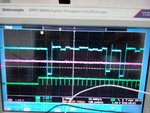
The simulation is being run my Proteus all fine, but in reality, the output of U1 when checked on scope this is what i get with no changes2.jpg

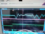
and when i tried shorting R4 this is what it became. 1.jpg

As u can see, the U2A has no effect on its output whatever the input is. Its neither saturated output nor 0. The output is fixed at 0.7V. I got populated another PCB card and the result was same in it too. Now can anyone please let me know, why is it so, moreover, if i bypass this SalenKey OpAmp and give the output of U1 to U1A's input, the gain works all fine.
 

Hi,

i see three lines on your scope picture.
What signals are these three lines?

Klaus
 

Blue one is the output of Difference OpAMp, pink one is the output of filter OpAmp and 3rd one is The ADC signal of conversion status
 

The reports are still rather mysterious. Your schematic shows input from a constant current source. Where does the varying input signal come, from apparently there's some kind of signal switching happening?

More generally speaking, I don't see how this kind of vague and incomplete information can substantiate a serious problem analysis.
 

Hi,

Your timing is 100us/ div?

Then you are way too fast switching your inputs.
You have a third order low pass filter with a settling time of maybe some 100ms.

Don´t fool us und use the same circuit in reality as shown in your picture.

Klaus
 
  • Like
Reactions: fouwad

    fouwad

    Points: 2
    Helpful Answer Positive Rating
Status
Not open for further replies.

Part and Inventory Search

Welcome to EDABoard.com

Sponsor

Back
Top