Continue to Site

Welcome to EDAboard.com

Welcome to our site! EDAboard.com is an international Electronics Discussion Forum focused on EDA software, circuits, schematics, books, theory, papers, asic, pld, 8051, DSP, Network, RF, Analog Design, PCB, Service Manuals... and a whole lot more! To participate you need to register. Registration is free. Click here to register now.

How to bias for differential amplifier?

Status
Not open for further replies.

anhnha

Full Member level 6
Full Member level 6
Joined
Mar 8, 2012
Messages
322
Helped
4
Reputation
8
Reaction score
4
Trophy points
1,298
Activity points
3,684
Hi.

I am designing a differential amplifier. Could anyone tell me how to to choose bias voltages, Vbias1, Vbias3 here?
What is the calculation needed to do?
Thanks.

103744d1396256179-differential-amplifier.png
 

Attachments

  • Differential amplifier.png
    Differential amplifier.png
    14.3 KB · Views: 548

Well I think we may need to know more about the application. The biasing voltages are obviously used to turn on the gates depending on what you are trying to compare and when the signal should be triggered or not. Vbias1 should be the level to activate the total amplifier and drive the PMOS low to turn them on. Vbias3 passes either V+ or V- depending on what you are comparing. For all this work, this seems like an easy job for an op-amp to do and looks similar to the internal structure of an op-amp.
 
  • Like
Reactions: anhnha

    anhnha

    Points: 2
    Helpful Answer Positive Rating
Hi.

Thanks for help.

Well I think we may need to know more about the application.
It is used for LDO with Vout = 2V.
. The biasing voltages are obviously used to turn on the gates depending on what you are trying to compare and when the signal should be triggered or not.
The output voltage is feedbacked to V+ and is compared with reference voltage V - = Vref = 1.5V.
Vbias1 should be the level to activate the total amplifier and drive the PMOS low to turn them on.

M2 acts as a current source. Then should I bias it so that it operates in saturation region?

Vbias3 passes either V+ or V- depending on what you are comparing. For all this work, this seems like an easy job for an op-amp to do and looks similar to the internal structure of an op-amp.

I need the output voltage swings between 0.2 and 2V.
How can I make a calculation for that?
 

... how to to choose bias voltages, Vbias1, Vbias3 here? What is the calculation needed to do?

You don't need to calculate: MOS bias voltages are created via current mirrors.

For Vbias1 add a constant current (CC) source from vdd to one more NMOS transistor, same W/L as M2, drain connected to its gate ("diode connection", similar to the PMOS M0); this gate voltage is your Vbias1. Choose the CC source value up to your needs (bandwidth), realize it by an isource (for simulation purpose only), in reality by a proper resistor, or by one more PMOS, gate connected to gnd or to an arbitrary fixed voltage between (vdd-vth) and gnd, e.g. by a resistor divider, with a W/L ratio which provides the required current. Don't use net59 for its gate voltage!

For Vbias3 use the same gate voltage Vbias1, but make M5 & M6 a factor of 2 smaller: W/L=1u/180n, because M3 .. M6 each get half the current of M1.
 
  • Like
Reactions: anhnha

    anhnha

    Points: 2
    Helpful Answer Positive Rating
Well, thanks a lot. I will try to simulate it now.
The circuit is from an IEEE paper attached below.
Here is the picture of the regulator with that amplifier included.
I want to ask for help to understand that circuit.

1. Do M10 and M11 need to be biased so that they act as resistors?
2. The paper says that the regulator is based on a folded cascode differential input stage with a current buffer compensation.
Could you point out where is the current buffer compensation?
What is its purpose?
3. Could you explain why did you choose the bias circuit like that?
4. What is the role of capacitor Cc in the picture?

103768d1396291079-regulator..png


P.S. Here is the bias circuit as you suggested. Could you confirm if it is correct or not?
Opps. I detected a mistake. M9 should be diode connected.

103770d1396293555-error-amplifier.png
 

Attachments

  • regulator..PNG
    regulator..PNG
    67.8 KB · Views: 339
  • A Fully Integrated HF-Band Passive RFID Tag IC using 0.18um CMOS Technology for Low-Cost Securit.pdf
    1.4 MB · Views: 203
  • Error amplifier.png
    Error amplifier.png
    16.6 KB · Views: 352
Last edited:

Hi anhnha,

You circuit is totally wrong .... where is the O/P node of your the amp that you are designing........ Please read singe ended differential amplifier, lots of materials are available over net.

Explaining the pic that you have attached from the IEEE paper:

1) The picture shows an LDO where
(a) The Mp is the Power FET (that will supply current to the load)
(b) The resistor divider is the feedback beta network
(c) The rest of the circuit is a folded cascode error amplifier (error amplifier is just a trans-conductance amplifier)
(d) Vg is the O/P node of the error amplifier

2) M10 & M11 must be in saturation. The gain of the error amplifier alone is approx = gm1 * (ro7 || gm*r09*ro11)

3) Cc acts as a compensation capacitor. This is used to maintain good phase margin (45 - 60 deg) for stability of the LDO.

Hope this will help .... :)
 
  • Like
Reactions: anhnha

    anhnha

    Points: 2
    Helpful Answer Positive Rating
Thank you, SH.

You circuit is totally wrong .... where is the O/P node of your the amp that you are designing........
Could you explain more? And what is O/P node?
(c) The rest of the circuit is a folded cascode error amplifier (error amplifier is just a trans-conductance amplifier)
This is the part that I don't quite understand.
(d) Vg is the O/P node of the error amplifier
It would be great if you could explain about O/P node.
Ah, did you mean "output node"?
2) M10 & M11 must be in saturation. The gain of the error amplifier alone is approx = gm1 * (ro7 || gm*r09*ro11)
May I know the reason? Why they should be in saturation?
I usually see M10 and M11 are replaced by resistors. What is wrong with that?
Here is what I understand about the role of parts in the circuit. Hope you could guide me where I am wrong.

1. M5: it is biased to operate as a current source.
2. M3 and M4: they together form "current mirror".
3. M1 and M2: differential amplifier.
4. M6 and M7: current mirror
5. M8 and M9: really can't get it, what is its function?
6. M10 and M11: they seems to be current sources (as you said)

Do you know any reference in which the circuit is analysed in detail?

Thanks.
 

1. Do M10 and M11 need to be biased so that they act as resistors?
No, they should operate in saturation mode in order to maintain good current regulation.

2. The paper says that the regulator is based on a folded cascode differential input stage with a current buffer compensation. Could you point out where is the current buffer compensation? What is its purpose?
It's the Cc capacitor. Its purpose is to reduce the unity gain bandwidth (UGB) of the amplifier, thereby increasing its phase margin (PM). Also, see SIDDHARTHA HAZRA's answer.

3. Could you explain why did you choose the bias circuit like that?
Because this is the standard method to bias CMOS circuits. An extensively constant current - often created via a band gap reference voltage - supplies current mirrors, which create the bias voltages. Currents can be easily divided or multiplied via the mirrors' W/L ratios.

4. What is the role of capacitor Cc in the picture?
See above!

Could you confirm if it is correct or not?
Opps. I detected a mistake. M9 should be diode connected.
Right!
 
  • Like
Reactions: anhnha

    anhnha

    Points: 2
    Helpful Answer Positive Rating
Hi.
In the picture of LDO from the paper, the paper says that the regulator is based on a folded cascode differential input stage . I see M1 and M2 form differential but could you tell me where is the folded cascode?
 

Could you explain more? And what is O/P node?

Yes I mean output node ...


The rest of the circuit is a folded cascode error amplifier (error amplifier is just a trans-conductance amplifier)
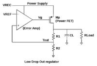


The simplified LDO circuit is attached with this post. There you can clearly see the error amplifier , the power FET, the feed back network.
The pic that you have uploaded from the IEEE paper is nothing but the complete inner circuit of the error amp, along with PFET & feed back network.

Working Principle: LDO is voltage regulator. It can supply current to the load and maintain constant voltage. (Basically it acts like a voltage source). When current is drawn from Vout then CL gets discharged and voltage a the the Vout drops. Now as the voltages at both the inputs of an error amplifier (like that of an op-amp) has to be same, so the loop drops the voltage Vg down so that Vsg of Power FET (Mp) increases and it can supply more current. This increase in current charges the CL and Vout increases back to the desired value.

Just type "understanding LDO" in google

I usually see M10 and M11 are replaced by resistors. What is wrong with that?

I will suggest you please read single ended differential amplifier, telescopic cascode amplifier & then folded cascode amplifier from any good book.
You may follow "Design of Analog CMOS Integrated Circuits, by B.Z.Razavi"

1. M5: it is biased to operate as a current source.
2. M3 and M4: they together form "current mirror".
3. M1 and M2: differential amplifier.
4. M6 and M7: current mirror
5. M8 and M9: really can't get it, what is its function?
6. M10 and M11: they seems to be current sources (as you said)

1. M5: it is biased to operate as a current source. ---- CORRECT
2. M3 and M4: they together form "current mirror". ----- CORRECT
3. M1 and M2: differential amplifier. ---------------------- CORRECT
4. M6 and M7: current mirror ------------------------------ CORRECT
5. M8 and M9: really can't get it, what is its function? ---------- They are the CASCODE MOSFET
6. M10 and M11: they seems to be current sources (as you said) ------ Yes they are

The M6 - M11 form the folded cascode structure. It will be clear if you read about it.

Hope this will help .... :)
 
  • Like
Reactions: subbu2 and anhnha

    anhnha

    Points: 2
    Helpful Answer Positive Rating

    subbu2

    Points: 2
    Helpful Answer Positive Rating
    V

    Points: 2
    Helpful Answer Positive Rating
I see M1 and M2 form differential but could you tell me where is the folded cascode?

M10, M11 represent the load transistors (CC loads in common base (CB) configuration) of the M1, M2 differential input stage. At these entry points, the differential signals are fed to the folded cascode differential stage M8, M9, - in CB config., too. M6, M7 are their load transistors, changing their differential signal via M6' diode connection into the single-ended output signal Vg for further amplification by the common source (CS) configured PMOS output stage Mp, which has to provide the required output current.

The expression folded results from the fact, that the PMOS CS input stage feeds their signals into an NMOS CB stage, thereby folding the original signal flow (downwards) into an upward direction.

Vout is defined by back-feeding a part of Vout (Vfb) equal to VREF: Vout = ((R1+R2)/R2)*VREF , for Vfb=VREF .
 
  • Like
Reactions: anhnha

    anhnha

    Points: 2
    Helpful Answer Positive Rating
Thank you, SH and Erikl, for the detailed explanations.
@SH: I understand LDO in general. However, my confusion is about the inner part of error amplifier.
@Erikl: Thank you. I ask to divide the circuit into small blocks and from that it will be easier to read and understand.
I would like to ask another question. The output of error amplifier is a current, right?
Vg will be equal to the current multiplied with the input impedance of PMOS output stage Mp.
 

Hi anhnha,

The output of error amplifier is a current, right?
Vg will be equal to the current multiplied with the input impedance of PMOS output stage Mp.

No the Vg node is a voltage node. You can see it is connected to the Gate of the PMOS Mp so there is no current output. The Vg node defines the Vsg for the PMOS (Mp).
But the output of the LDO i.e. Vout, will give both voltage and current output.

Take an example: In my previous post I have attached a diagram of an LDO. You can see there is a load resistance (Rload). Say the output of your LDO is 2V and Rload is 20Omhs.
Then the current output is 100mA. The loop will adjust Vg such a way that the Vsg of the PMOS (Mp) is sufficient for it to provide 100mA at steady state.

Hope this will help ... :)
 
  • Like
Reactions: anhnha

    anhnha

    Points: 2
    Helpful Answer Positive Rating
Hi again.

Could you tell me a systematic method to bias the circuit so that all necessary transistors are in saturation.

103768d1396291079-regulator..png


I chose Vbias1, Vbias2, and Vbias3 all above the threshold voltage of NMOS transistors a little and therefore, M5, M8, M9, M10, and M11 all are in saturation. However, the problem here is that all the rest transistors are NOT in saturation.

M3: Saturation GOOD
M4: Linear: WRONG.
M1: Subthreshold: WRONG
M2: Subthreshold: WRONG.
M6: Saturation: GOOD
M7: Saturation: GOOD
M8: Subthreshold: WRONG.
M9: Subthreshold: WRONG.
Mp: Saturation: GOOD

All these transistors should be in saturation but I can't figure out how to do that.
Please help me out.
 

I chose Vbias1, Vbias2, and Vbias3 all above the threshold voltage of NMOS transistors a little and therefore, M5, M8, M9, M10, and M11 all are in saturation. However, the problem here is that all the rest transistors are NOT in saturation.
...
All these transistors should be in saturation but I can't figure out how to do that.

Again: Vbias1 = Vbias3 , but in this circuit, in contrary to what I suggested above, for M10 & M11 don't use a smaller W/L (this suggestion was for a different circuit), but the same as for M5 or even a 50% larger W/L , because in this circuit, the current of 2 branches have to be sunken.

Vbias2 is critical, it depends on VREF . If you need further help, show the circuit diagram with voltage values at all the nodes.
 
  • Like
Reactions: anhnha

    anhnha

    Points: 2
    Helpful Answer Positive Rating
Hi anhnha

You can bias folded cascode opamp as an attached picture. Every transistor in SATURATION (Note: I do not have mp transistor in your picture) I will add mp to design LDO later.

 
Thank you, Erikl and tompham.

Erikl:
If you need further help, show the circuit diagram with voltage values at all the nodes.
Yes. I will post it later. At present, I use ideal dc source to bias. I need to replace it by a biasing circuit.
tompham:

Thanks. I will try it now.
 

Hi.
This is my circuit with node voltages.
I drew the circuit as tompham's but all transistors except M12 are in subthreshold. M12 is in linear.
 

Attachments

  • LDO.png
    LDO.png
    18.7 KB · Views: 342

Hi anhnha

Your nmos M10 should m = 4 instead of m = 1
 
  • Like
Reactions: anhnha

    anhnha

    Points: 2
    Helpful Answer Positive Rating
Evn I am designing an LDO with following specs..
Vin : 1.8V +/- 10%
Vout : 1.5V +/- 3%
Vref : 1V +/- 1%
Iload : 0 to 50mA
Ext Cap : 100nF +/- 20%
PSR : >40dB upto 10MHz

Can anybody please explain me which method is better whether to proceed block by block like designing error amp then moving on to power mosfet etc...or whether to simulate the whole LDO circuit and then analyse..

please suggest me the way forward..I have read abt the Single stage diff amp and abt miller compensation after adding second stage and yet to start wit the design.
 
Last edited:

Status
Not open for further replies.

Part and Inventory Search

Welcome to EDABoard.com

Sponsor

Back
Top