Continue to Site

Welcome to EDAboard.com

Welcome to our site! EDAboard.com is an international Electronics Discussion Forum focused on EDA software, circuits, schematics, books, theory, papers, asic, pld, 8051, DSP, Network, RF, Analog Design, PCB, Service Manuals... and a whole lot more! To participate you need to register. Registration is free. Click here to register now.

Buffer hardware between oscilloscope probe and sound card line in

Status
Not open for further replies.

boylesg

Advanced Member level 4
Joined
Jul 15, 2012
Messages
1,023
Helped
5
Reputation
10
Reaction score
6
Trophy points
1,318
Location
Epping, Victoria, Australia
Visit site
Activity points
11,697
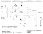
buff.gif
http://xoscope.sourceforge.net/hardware/buff.gif

The author does not explicitly specify where the ground wire of the sound card 'line in' should be connected.

If I were to have a guess I would say that it would be the GND associated with the RCA connector.

Would this be correct?
 

What signal freq you plan to measure ?

15 - 20kHz

Already tried it with a very simple voltage divider and it worked, although the signal was a bit distorted as it looked more like a sine wave than a square wave.

I am wondering if this buffer circuit will produce a better signal for me.
 

boylesg, did you compennsate the voltage divider? This where you put a small variable capacitor across the "top" resistor" to compensate for the capacitance from the CRO input + cable which is across the "lower" resistor. As an example, suppose the "top" resistor is 100K and the lower resistor is 10 K to make a 10 -1 divider. the 10 K will have ths CRO input capactance across it- 50 pF? + the lead capacitance - 200 pF?, giving a total of 250 pF, the 100K then needs 250/10 = 25 pf across it. This should be a fixed cap of 15 pF + a variable 3-30 pF. This cap it adjusted using the "cal" output of the CRO to get the best square on the display.
Frank
I haven't implemented it yet, just trying to figure it out at present before proceeding to do it on a bread board. Only just sorted out a negative 12V source - an ATX power supply with some salvaged connector pins from a tv circuit board jammed into the appropriate contacts on the ATX motherboard plug.
-12V, 0, +12V and also -5V, 0, +5V. Will save me frigging around with a 555 based negative voltage generator on my bread board.

And I don't have an real oscilloscope as present, only a multimeter. Any reference to an oscilloscope has been in reference to the virtual one in multisim 11.

I have read else where, where people have made cro probes, that the x10 and x1 probes are either seperate with different resistors in them or one probe with a switch that changes between two different resistors. This guy has all the resistors in his circuit board.

Hence the probes can be a simple multimeter type ones? Also is it really necesarry to use coaxial cables, with RF shielding and all that, when you are measuring strong voltages and currents such as 12V, 15mA?

- - - Updated - - -

Some things about this circuit that are not clear to me.

C1: .001uF
I understand this is to stop DC and only allow AC to pass. But if you are trying to measure pulsed DC current or just straight DC current?

R5 and R4 on the opamp.
I get R4 - it is just forms a bog standard non-inverting amplifier with the opamp.
But I don't get R5 connected to ground. Is it meant to short R4 when the switch is thrown? If so then what does the non-inverting amplifier become? Is a grounded inverting input pin another way of implementing a non-inverting amplifier?
 

Your project is located here:

Buffer Hardware for xoscope
http://xoscope.sourceforge.net/hardware/hardware.html

buff.gif


Circuit Description
http://xoscope.cvs.sourceforge.net/viewvc/xoscope/xoscope/hardware/HARDWARE?revision=HEAD

Code:
	Sound card buffer circuit (buff.fig) for use with [x]oscope

	by Tim Witham <twitham@pcocd2.intel.com>


	NO WARRANTY

THIS CIRCUIT IS PROVIDED "AS IS" WITHOUT WARRANTY OF ANY KIND, EITHER
EXPRESSED OR IMPLIED, INCLUDING, BUT NOT LIMITED TO, THE IMPLIED
WARRANTIES OF MERCHANTABILITY AND FITNESS FOR A PARTICULAR PURPOSE.
THE ENTIRE RISK AS TO THE QUALITY, PERFORMANCE AND SAFETY OF THE
CIRCUIT IS WITH YOU.


	HISTORY

I was probing a circuit with a piece of wire to the line in on my
sound card when I happened to notice that the probing was loading my
circuit down.  This implies my sound card's line input may have less
than ideal input impedance for looking at arbitrary signals.  I
eliminated the loading by using a less intrusive 10x (10 times)
attenuating oscilloscope probe.  But then the signal was too small to
see on [x]oscope.  So, for fun, I actually built a little line in
buffer circuit to solve these problems and more.


	THE BUFFER CIRCUIT

The result is shown in the file buff.fig (xfig source format) or
buff.ps (postscript format).  The purpose of this circuit is to:

1) Look like a real oscilloscope to the circuit under test.  That is,
to have an input impedance of 1 Megohm in parallel with 20 pF.

2) Have a x1 / x10 switchable amplifier to produce the same amplitude
with 1x and 10x probes respectively.

3) Provide a line level trim control for adjusting the amplitude to an
optimum level for the sound card's input.

4) Provide high voltage protection to the sound card and PC for those
times when you accidentally probe your 60Hz line-voltage AC!

The circuit accomplishes these goals.  It is adapted from part of a
circuit shown in figure 4.74 of the excellent book "The Art of
Electronics" by Paul Horowitz and Winfield Hill, 2nd ed., 1989.  Most
of the parts can be purchased at your local electronics store for
under $30.00; see the parts list below.  Two identical circuits are
built, one for each of the sound card's left and right line inputs.


	CIRCUIT EXPLANATION

C1 is for AC coupling to remove any DC first.  R1 and C2 set the input
impedance seen by the circuit.  In retrospect, C1 should probably have
been on the other side of R1 and C2 so as to not affect the input
impedance at all.  But it seems to work fine this way too.

D1, D2 and R2 limit the input voltage to the range -12V to 12.7V for
the high voltage input protection.  R2 must be 1/2 Watt for 150 Volt
protection.  D3 and R3 produce a clamp voltage at -11.3V to keep the
op-amp in common mode range.

The TL082 is a dual JFET input op-amp providing the necessary high
input impedance.  A similar JFET input part may work just as well.
R5, R4 and S1 provide the x1 or x10 amplification.

Finally, R6 is used to trim the output to an acceptable level for the
soundcard. It can be brought all the way down to ground to get the
same effect as the "GND" input coupling of a real oscilloscope.


	ASSEMBLY AND CONNECTION

See buff2.fig or buff2.ps for my circuit layout.  I built two of the
circuits on the back of a full size drive bay cover.  The op-amp and
surrounding components were mounted on a small circuit board (see
pcb.fig / pcb.ps) positioned in the center of the drive bay cover.
The BNC connectors, switches and potentiometers were mounted through
the cover on either side of the circuit board.  The result is under
1/2" thick so an internal drive can even fit behind it.

A -12V power connector may not be readily available in your computer.
The standard disk drive power connectors are +5 and +12.  I added an
alternate power connector in my system by tapping my power supplies'
-12, GND, and +12 wires.  Be careful not to get these mixed up!

Finally, I used a Y adapter cord to connect the two phono jacks to the
1/8" stereo line input on the sound card.


	PARTS LIST

Qty	Part#	Description

1	IC1	TL082 Dual JFET input operational amplifier

2	R1	1M,	1/4 Watt, 5% resistor
2	R2	47k,	1/2 Watt, 5% resistor
2	R3	4.7k,	1/4 Watt, 5% resistor
2	R4	3k	1/4 Watt, 5% resistor
2	R5	27k,	1/4 Watt, 5% resistor
2	R6	100k,	linear potentiometer

2	C1	.01uF, 1kV	ceramic disc capacitor
2	C2	20pF		ceramic disc capacitor
2	C3	100pF		ceramic disc capacitor

6	D1-D3	1N914 or 1N4148 silicon switching diode

2	S1	SPST mini toggle switch

1		circuit board, (1/2 RS 276-159)
1		8-pin DIP socket
2		1/4" knob for R6
2		female BNC connectors, panel mount
2		female RCA connectors, in-line type
		tap-in and power connectors
		connecting wire, power wire


	DISCLAIMER

This circuit was designed and built by me on my own time and
equipment.  My employer has absolutely nothing to do with it.


If you have comments on this thing, please let me know.

	Tim Witham <twitham@pcocd2.intel.com>
 

1) Trimmer is the output voltage level; it can vary the output level from 0 to 100% of the input level or from 0 to 1000% of the input level (depending on whether the S1 gain switch is off or on).
2)When the input voltage goes over +12.6V or below -12.6V the appropriate diode conducts and shunts the current (coming through R2 or C3) from any big voltage error into the power supplies, not into your op amp.


What is the 1:1 and 10:1 component in the circuit spec? I don't recognize the symbol.

What are the signficant advantages of this buffer circuit over the one I previously found?

Also what is the advantage, if any, of producing negative voltage this way compared to producing one via a 555 timer? Greater amperage?
 

I notice this design has a means of allowing DC through the input capacitor if desired.

Have been wondering about that.

With the circuit I found there is no means of doing this but I could easily add something I suppose.

If I was trying to measure an oscillating 555 signal with the sound card input buffer I found then I can't see that the signal would pass the input capacitor. Only AC current can pass a capacitor as I understand it.
 

This design is made for a 10MΩ 2pF probe so that it can be matched with vbl. cap on probe.for square wave response. Probe attenuates 10:1 and then gain= 1+9 =10 with AC coupling which can be bypassed on some PC audio designs for DC restore circuits using FET buffered mic. Similar design of FET buffered Probe with x10 gain can also be DC coupled on certain PC's HPF is limited by GBW product of Op Amp so with gain of 9 , adequate BW for audio . AC hum may be possible with 100KΩ pot source impedance and poor CMMR noise rejection. CM choke is best advice, as well as careful ground from PC AC input thru case to RCA jack to BNC jack.I would prefer to see <1KΩ source impedance. to reduce noise issues.

As a measure of noise floor, Cool Edit Pro2 mic noise floor can reach -70dB on a great system, -40dB on a poor system and -30dB if really noisy. 0dB is clipping. How would this design compare on spectral noise? of ground with probe to ground.
 
  • Like
Reactions: tpetar

    tpetar

    Points: 2
    Helpful Answer Positive Rating
@boylesg

My friend, I have one question. Do you try to make scope for home usage or goal is to use sound card for that purpose ?

What Jedi skills/expirience you have with soldering iron and making good PCB ?
 
Last edited:

The goal is to create a PC scope using my existing sound card. At this stage I am not willing to fork out about $200 for commercial PC oscilloscope and besides, these simple buffer circuits look like a fun little learning exercise.

I have already tried the sound card line in with a simple voltage divider on my 555 timer circuit and was able to see the oscillation through Virtual Analyser. Although it looked like a sine wave rather than the expeted square wave. Hence I have moved up to this slightly more complicated buffer circuit to see if I can get a better signal.

I am not far off a raw beginner with this stuff but I have learned a few basic concepts and electronic building blocks. Many gaps to fill in yet however.

I have been using the prototype boards. Have not bothered with PCB etching as yet. For these simple circuits the prototype boards are good enough I reckon.

Skill with a soldering iron? You mean like not getting stray solder blobs all of the place and making stray electrical connections? Got myself a quite small USB soldering iron for any particularly fiddly bits, e.g. 555 timer.

- - - Updated - - -

With this AC coupling thing......am I taking it too literally in meaning that only AC (as in both negative and positive oscillations) can pass?

Or can the positive oscillations produced by a 555 also pass through the coupling capacitor by virtue of charging it up and then allowing it to discharge into the buffer circuit on the down cycle of the 555.

So any steady voltage is blocked by the AC coupling capacitor but any variations above or below that steady voltage are passed into the rest of the buffer circuit?
 

I ask you because I have some nice scope project for you if you whant just to make some scope. But some soldering SMD skills are needed to assemble this, also uC programming and good PCB making, all this is needed. Scopes are PC and standalone with big nice GLCD for few MHz.
 

Oh OK.

I have come across a diy stand alone usb oscilloscope based on a PIC chip but it was rather complicated circuitry and felt I was not up to it just yet. Perhaps this is the one you are refering to, or similar.

Let me get my head around this simple buffer circuit, get it soldered up, use it for a while, build my general electronics knowledge and then I may feel ready for this more complicated PC oscilloscope.

At this stage I just want to be able to visualise the signals but not necessarily take accurate measurements of them with the oscilloscope. I have purchased a pretty good DMM for accurate measurements.

This one in fact: **broken link removed**

The seem to retail for about $120 so I reckon I have done pretty well.

I much prefer to have some level of understanding the circuit I am building rather than just building it blind.
 

R5 and R4 on the opamp.
I get R4 - it is just forms a bog standard non-inverting amplifier with the opamp.
But I don't get R5 connected to ground. Is it meant to short R4 when the switch is thrown? If so then what does the non-inverting amplifier become? Is a grounded inverting input pin another way of implementing a non-inverting amplifier?

S1 open = X1 amp. S1 closed = X10 amp.

When switch is open, op amp output is fed to negative input through R5 ohm resistor. Op amp inputs draw negligible current, voltage drop across R5 is virtually 0, and negative op amp input gets output voltage, thus op amp is a unity gain follower when S1 is open.

When switch is closed, R4/R5 serve as a 10:1 voltage divider (pulling down through ground). Op amp output travels through 270k resistor then 30k resistor to ground, so negative op amp input gets 1/10th output voltage, and op amp becomes an x10 (20db) gain amp.

See https://www.allaboutcircuits.com/vol_3/chpt_8/5.html for good explanation with pictures.

If I were to have a guess I would say that it would be the GND associated with the RCA connector.

Would this be correct?

And yes that is correct. This buffer is just one channel; you can tie the ground and right channel on the sound card line in together and to your signal ground (0v on your amp supply) and run it as a mono input to sound card; commonly available mono rca -> 1/8inch trs cables / adapters (e.g. https://www.musiciansfriend.com/accessories/hosa-rca-female-to-mono-1-8-adapter) will do this for you. See https://en.wikipedia.org/wiki/TRS_connector#Mono_and_stereo_compatibility.

Bummer that atx doesn't have a standard negative rail output connector aside from the motherboard, would make it easy to power your amp off the host machine -- the ide connectors are only +12/+5/GND. :/

J
 
Last edited:

Status
Not open for further replies.

Part and Inventory Search

Welcome to EDABoard.com

Sponsor

Back
Top