Continue to Site

Welcome to EDAboard.com

Welcome to our site! EDAboard.com is an international Electronics Discussion Forum focused on EDA software, circuits, schematics, books, theory, papers, asic, pld, 8051, DSP, Network, RF, Analog Design, PCB, Service Manuals... and a whole lot more! To participate you need to register. Registration is free. Click here to register now.

12-way resistive splitter layout

Status
Not open for further replies.
Thanks a lot again Volker! I guess data is good enough to try it on PCB (I am looking at https://www.edn.com/electronics-blo...ch-return-loss-is-too-much--Rule-of-Thumb--12 as a reference for S11 vs S21 as below). As for trace width - I double checked with all CPWG Ground calculators available and all of them show impedance in a range 50-51 Ohm for FR4 0.6mm, two layer, 0.65mm trace width, 0.2mm gap, so can I assume that this is FR4 substrate contributes to S11 (path from input port to the first resistor)?

THANKS AGAIN!

- - - Updated - - -

Thanks a lot Volker! Data looks good - I am using the following reference ( https://www.edn.com/electronics-blo...ch-return-loss-is-too-much--Rule-of-Thumb--12 ) to get a sense how much S11 is too much (see graph below), and based on this data 8-port design has a good chance to be implemented. As for trace width (quote: "According to my simulation the line width isn't correct, this is what I get for the path from input port to the first resistor" ), I double checked with all available CPWG Ground calculators, and looks like my calculation is correct - for two layer 0.6mm FR4 with 0.51mm substrate height, trace 0.65mm and gap 0.2mm CPWG Ground shows 50-51 Ohm impedance, so it's probably FR4 contributing to S11 the most (I guess). I will go ahead and order PCBs for both designs and see how it will perform in real world. Just in case you will have a chance to try my 12 port stuff - it will be really appreciated. Good stuff! Thanks again!
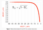
S11vsS21.png
 

On the other hand, I just had a lengthy chat with my "RF reference" Kent Britain, and he reminded me that FR4 has 4.6 Err measured (usually) at 100 MHz, and at 6GHz it is more likely 3.8-3.9. When we deal with Rogers or alike, their Err is the same on a wide frequency range. So. having this in mind, and paying a bit with Saturn microstrip menu, one can figure out effective Err, and after taking it and placing in CPWG menu as a reference, it looks like my gap in CPWG Ground calculation should be something around 0.15mm (not 0.2mm as previous) to show better results in 2-6 GHz range. Thanks to Volker again for flagging something fishy about the trace - all leads to conclusion that slightly tighter gap should improve S11. Below are updated gerbers:

View attachment Gerber_1-to-8-resistive-splitter_20190427184710.zip

View attachment Gerber_1-to-12-resistive-splitter_20190427184805.zip
 

My usual value for FR4 in the GHz range is eps_r=4.3. From my analysis of a separate straight line segment, using eps_r values of 4.3 to 4.6, the line width should be increased to 800µm with a gap of 150µm.

To double check if the issues with the (initial) full model are indeed caused by the lines, I created a separate testbech for the "core only" model excluding the feedline. Those results look much better indeed:

result_core_only.jpg

testbench_core_only.jpg
 
  • Like
Reactions: alftel

    alftel

    Points: 2
    Helpful Answer Positive Rating
Fantastic! The only thing that hunts me is that any CPWG Ground calculator that I punch this data in does not produce 50 Ohm impedance (i.e. 0.51mm substrate height, 0.65mm trace width, 0.15mm gap, FR4 Err = 4.3). The best results that I see so far (based on data references below) are: Err = 4.0, trace width = 0.65mm, gap = 0.12mm, height = 0.51mm

Which tool are you using for CPWG with Ground line impedance calculation? I have no doubt that your tool(s) is no match to whatever is available free on a web, just trying to understand why results are so different, and should I trust TXLine or Saturn PCB going forward. What kind/size of gap your tool will give with Err = 4 an trace width = 0.65mm?

CPWG Ground Calculators:

1) TXLine
2) Saturn PCB Toolkit
3) http://www.wenshing.com.tw/Design_tools/Coplanar-Waveguide-with-Ground-Calculator_e.html
4) http://chemandy.com/calculators/coplanar-waveguide-with-ground-calculator.htm
5) http://wcalc.sourceforge.net/cgi-bin/coplanar.cgi
6) http://www.changpuak.ch/electronics/Coplanar_Waveguide_Calculator.php
7) http://www.rfdh.com/rfdb/cpwg.htm
etc. etc.

Here are references to FR4 high frequency Err:

1) http://www.polarinstruments.com/support/cits/AP155.html
2) **broken link removed**
3) http://blog.rogerscorp.com/2011/03/16/when-digital-signals-reach-microwave-frequencies/
4) http://www.isola-group.com/wp-content/uploads/Making-Sense-of-Laminate-Dielectric-Properties.pdf
5) http://resources.altium.com/pcb-design-blog/everything-you-need-for-successful-pcb-stackup-design

etc. etc.
 

Which tool are you using for CPWG with Ground line impedance calculation?

I used my EM simulation tool (ADS Momentum) with a 15mm long segment of your line, including the actual vias at the actual via spacing.

linesegment.jpg

What is not included is solder resist.

But if you have good experience with the cross section solvers, that's fine with me. I used the same tool for the line that I also used for the "full model".

Regarding FR4 eps_r: there is no standard recipe hot to make FR4, which means there is no standard values, and results depend on the resin/fibre mixture. See page 6 here: https://www.we-online.de/web/de/ind..._1/signalintegritaet/Webinar_Signal_final.pdf
Even worse, the material is anisotropic and inhomogenous, so you will find different values for coupled lines (field in x-y plane) vs. microstrip resonators (field in z-direction) vs. 3D resonators (bulk average). For Isola material (low eps_r in your reference) we had indeed a very different result for our prototyping FR4 (Bungard, measured eps_r = 4.6).
That's one of the reasons to use a more tightly specified material when eps_r matters ... there are some affordable materials in between "unknown FR4" and "high end materials" like Rogers.
 
Last edited:
  • Like
Reactions: alftel

    alftel

    Points: 2
    Helpful Answer Positive Rating
Thanks Volker! Danke Schön! I didn't know that vias and their respective spacing contribute to this calculation - always learn something.... I am a dumb person more or less when it comes to topics where I am not 100% certain, and do listen to experience and advice (like yours). Desirable trace width of 0.65mm is dictated by the fact that 0402 packaging pads are 0.65mm wide, plus 0.65mm trace nicely fits between ground pads of MMCX connector to the pin. So, assuming that I still do desire to maintain 0.65mm trace width, what would be suitable gap to bring impedance to 50 Ohm as close as possible in my case?
 

The 800/150 was my choice to avoid tolerance issues with narrow gaps.

I didn't know that vias and their respective spacing contribute to this calculation

I never checked how much effect that is, but I have more trust in my 3D model than 2D cross section model with "ideal" connection between side ground and backside ground. On the other hand, my simulation doesn't include solder resist, which adds some capacitance to the side grounds.

Maybe you just leave your values and see what you get. The important part is: the "core divider" looks good in simulation!
 
  • Like
Reactions: alftel

    alftel

    Points: 2
    Helpful Answer Positive Rating
Status
Not open for further replies.

Part and Inventory Search

Welcome to EDABoard.com

Sponsor

Back
Top