Continue to Site

Welcome to EDAboard.com

Welcome to our site! EDAboard.com is an international Electronics Discussion Forum focused on EDA software, circuits, schematics, books, theory, papers, asic, pld, 8051, DSP, Network, RF, Analog Design, PCB, Service Manuals... and a whole lot more! To participate you need to register. Registration is free. Click here to register now.

[Moved]: S-parameter measurement simulation

Status
Not open for further replies.

promach

Advanced Member level 4
Joined
Feb 22, 2016
Messages
1,202
Helped
2
Reputation
4
Reaction score
5
Trophy points
1,318
Visit site
Activity points
11,643
multiply by 2 using an E source

Anyone have any knowledge on how is the above implemented in s-param.cir ?
**broken link removed**

E2 7 0 6 0 2 $ amplify out port ac voltage by 2

http://paste.ubuntu.com/25573616/ --> s-param.cir

I could not form any draw-able AC voltage source from this line of netlist. Could anyone help ?


Code:
Test for Scattering Parameters
** Two ports
** Examples: Bipolar,  Tschebyschef, RC

.param Rbase=50 Vbias_in=0 Vbias_out=0

*** The two-port circuit: 
** port 1: in 0
** port 2: out 0
** Bias on both ports through resistor Rbase (to obtain operating point)

** Example RF Bipolar mrf5711
** VCE 1 V, IE = 5mA
** QXXXXXXX nc nb ne
** model obtained from
** http://141.69.160.32/~krausg/Spice_Model_CD/Vendor%20List/Motorola/Spice/RFBJT/
*.include MRF5711.lib
*XMRF5711 out in e  MRF5711
*Ie e 0 5m
*Ce e 0 1

** Example Tschebyschef Low Pass filter
C1 in 0 33.2p
L1 in 2 99.2n
C2 2 0 57.2p
L2 2 out 99.2n
C3 out 0 33.2p

** Example RC
** see
** http://www.allenhollister.com/allen/files/scatteringparameters.pdf
*R2 in out 10
*C1 out int5 30p
*R1 int5 0 10

*** End of circuit


** The following subcircuit to be changed only by an experienced user!

*** Driver and readout
X1 in out S22 S12 S_PARAM

.SUBCKT S_PARAM 22 66 5 7
* Resistors emulate switches with Ron=0.001 and Roff=1e12
* to switch driver to input and readout to output (and vice versa, see below)
RS1 22 2 0.001
RS2 66 6 0.001
RS3 22 6 1e12
RS4 66 2 1e12
*Driver
Vacdc 1 0 DC 'Vbias_in' AC 1 $ ac voltage and dc bias at input (applied through load resistor)
R1 1 2 'Rbase'
E1 3 0 2 0 2       $ amplify in port ac voltage by 2
Vac 3 4 DC 0 AC 1  $ subtract driving ac voltage
R_loop 4 5 0.001
R3 5 0 1           $ ground return for measure node 5
*Readout
E2 7 0 6 0 2       $ amplify out port ac voltage by 2
R4 6 8 'Rbase'     $ load resistor at output (ac)
Vdc 8 0 DC 'Vbias_out' AC 0 $ dc bias at output (applied through load resistor)
.ends

** Check the two ac lines below for being equal!
.control
set noaskquit
set filetype=ascii
*** measurement for s11 and s21
op
** save bias voltages to vector
let Vdcnew=V(X1.1) $ former Vacdc 
let Vacdcnew=v(X1.8) $ former Vdc 
** first ac measurement (change this line only together with following ac line)
*ac lin 20 0.1G 2G $ use for bip transistor
ac lin 100 2.5MEG 250MEG $ use for Tschebyschef 
*ac lin 101 1k 10G $ use for RC
** 
** switch input and output
alter R.X1.RS1=1e12
alter R.X1.RS2=1e12
alter R.X1.RS3=0.001
alter R.X1.RS4=0.001
** switch bias voltages between in and out
alter V.X1.Vacdc DC=op1.Vacdcnew
alter V.X1.Vdc DC=op1.Vdcnew
*** measurement for s12 and s22
op
** second ac measurement (change this line only together with ac line above)
*ac lin 20 0.1G 2G $ use for bip transistor
ac lin 100 2.5MEG 250MEG $ use for Tschebyschef 
*ac lin 101 1 10G $ use for RC 
**
let s11=ac1.s22
let s21=ac1.s12
settype s-param S11 S21 S22 S12

let S11db = db(s11)
let S12db = db(s12)
let S21db = db(s21)
let S22db = db(s22)
settype decibel S11db S21db S22db S12db

let P11=180*ph(s11)/pi
let P21=180*ph(s21)/pi
let P22=180*ph(S22)/pi
let P12=180*ph(S12)/pi
settype phase P11 P21 P22 P12

let Rbase=@R.X1.R4[Resistance]
settype impedance Rbase

*plot s11db s21db S22db S12db ylimit -50 0 xlog $ used with RC 
plot s11db s21db S22db S12db ylimit -0.5 0 $ used with Tschebyschef  
plot P11 P21 P22 P12
plot smithgrid S11 S12
*wrdata s3046 mag(S11) P11 mag(S21) P21 mag(S22) P22 mag(S12) P12 $ write simple table
wrs2p s3046.s2p $ write touchstone vers. 1 file s3046.s2p
.endc

.end
 

Re: S-parameter measurement simulation

The bias voltages at the input and output ports of the circuit are set as parameters as well:

.param Vbias_in=1 Vbias_out=2


Vbias_in and Vbias_out are two parameters to be modified by user in s-param.cir.

I understand U0 = 1V, but why U2 = 2V ?
 

The following plots are obtained by running s-param.cir

U0 = 1V, U2 = 2V --> are these parameters set correctly ?

s_parameter_plot.png

smith_chart_plot.png
 

The 2V in the controlled source also makes sense. If I understand the netlist correctly, the 50 Ohm source is created by an ideal source + 50 ohm series resistor. This gives 1V output for 50 Ohm external load.
 

R1 1 2 'Rbase'

this 50 ohm Rbase is connected to the netlabel 2 in the screenshot below.

Or did I misread the s-param.cir netlist ?

Screenshot from 2017-09-22 11-12-46.png
 

OK. Now I am trying to understand the subcircuit before proceeding to the measurement section.
How should E1 and E2 be interpreted ?

Code:
X1 in out S22 S12 S_PARAM

.SUBCKT S_PARAM 22 66 5 7
* Resistors emulate switches with Ron=0.001 and Roff=1e12
* to switch driver to input and readout to output (and vice versa, see below)
RS1 22 2 0.001
RS2 66 6 0.001
RS3 22 6 1e12
RS4 66 2 1e12
*Driver
Vacdc 1 0 DC 'Vbias_in' AC 1 $ ac voltage and dc bias at input (applied through load resistor)
R1 1 2 'Rbase'
E1 3 0 2 0 2       $ amplify in port ac voltage by 2
Vac 3 4 DC 0 AC 1  $ subtract driving ac voltage
R_loop 4 5 0.001
R3 5 0 1           $ ground return for measure node 5
*Readout
E2 7 0 6 0 2       $ amplify out port ac voltage by 2
R4 6 8 'Rbase'     $ load resistor at output (ac)
Vdc 8 0 DC 'Vbias_out' AC 0 $ dc bias at output (applied through load resistor)
.ends
 

I am stucked at visualizing E1 which purpose is to amplify in port ac voltage by 2

Any idea ?

Screenshot from 2017-09-25 14-03-34.png
 

E1 3 0 2 0 2 $ amplify in port ac voltage by 2

This line means multiply the node voltage at #2 by a factor of two and the resultant voltage appears at node #3


Vac 3 4 DC 0 AC 1 $ subtract driving ac voltage

I do not understand this line though. Anyone ?
 

Vac 3 4 DC 0 AC 1 $ subtract driving ac voltage

That means you have an AC voltage source between node 3 (+) and 4(-) within a 0V DC component and a 1V AC component.

- - - Updated - - -

That means you have an AC voltage source between node 3 (+) and 4(-) within a 0V DC component and a 1V AC component.

Sorry for the double post i did not found out any modify option. I just want to add "Vac" is only a label, you could name your voltage source V1 or Vxy.
 

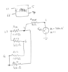
By implementing the 2-volt generator as two 1-volt generators—VG1A and VG1B in series with the generator resistance RG1 as shown—we achieve the particularly simple result that the voltage at node 11 is the reflected or scattered wave b1. Since a1 equals one, this is S11 itself

I do not understand the above statement.

Why must RG1 be between S11 and VG1A ?

Note: Screenshot extracted from **broken link removed**

S_Parameter_circuit.png

View attachment CreateS-ParameterSUBCKTinPSpice.pdf
 

Status
Not open for further replies.

Similar threads

Part and Inventory Search

Welcome to EDABoard.com

Sponsor

Back
Top