Continue to Site

Welcome to EDAboard.com

Welcome to our site! EDAboard.com is an international Electronics Discussion Forum focused on EDA software, circuits, schematics, books, theory, papers, asic, pld, 8051, DSP, Network, RF, Analog Design, PCB, Service Manuals... and a whole lot more! To participate you need to register. Registration is free. Click here to register now.

why the transient and DC analyses yields different results on Ibias generator circuit

Status
Not open for further replies.
I didn't understand this and I think that's the reason I'm having a difficulty on plotting the data. I did include these codes the .print vdb(n5) vdb(n3). AOL(dB) = N5(dB) - N3(dB). Is this correct? I inserted the "vn1 vn1 gnd dc 0V ac 1V" at the positive input of the OP.
not sure what simulator are you using? if spectre use
dB20(V(VN5) / (V(N1)-V(N3)))
phase(V(N5) / (V(N1)-V(N3)))
for eldo just plot
V(N5) / (V(N1)-V(N3))
it will give both magnitude in dB and phase automatically

your source has to break the wire not drive it, it should be something like
vn1 n1 n1_old dc 0V ac 1V
where you rename all other previous n1 nodes as n1_old except for the opamp input which is still n1

But right now it does not matter (at least not to solve your problem)...
... I finally noticed that your N1 and N3 do track nicely so gain was there, I misunderstood post #8 where you described N1 and N3 behavior I thought they were at different voltages

Congratulation Leo_o2, the new plots show clearly a second OP, now it is just a question of stabilizing the loops, a good cap in the right place will probably do the trick...

I guess allennlowaton you can try that next to see how your loop gain looks in the circuit, just break the output wire instead of the input one and look at
L=v(n5_opamp)/v(n5)
after inserting
vn5 n5 n5_opamp dc 0V ac 1V
and connecting the opamp output to n5_opamp instead of n5
do this at the OP where you see the oscillation

The circuit apparently still works but you'll like it better w/o the ringing, I'm sure
 
Last edited:
  • Like
Reactions: allennlowaton

    V

    Points: 2
    Helpful Answer Positive Rating

    allennlowaton

    Points: 2
    Helpful Answer Positive Rating
Thank you very much leo_o2.
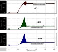
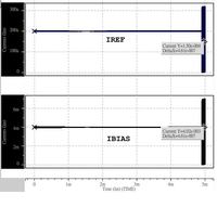
Here is the simulation result of your suggestion.


The problem has been solved though that peaking of up to 240uA(MN1) and more than 15mA(Mn2 and Mn4) bothers me.

A big thanks to dgnani, LvW and billichip.
 

For next step, you need to improve loop stability. It shows many rings in the waveform.
It is not easy to compensate this structure for all operating condition. However, it can be achieved to choose suitable structure of OPb.
 
not sure what simulator are you using? if spectre use
dB20(V(VN5) / (V(N1)-V(N3)))
phase(V(N5) / (V(N1)-V(N3)))
for eldo just plot
V(N5) / (V(N1)-V(N3))
it will give both magnitude in dB and phase automatically

your source has to break the wire not drive it, it should be something like
vn1 n1 n1_old dc 0V ac 1V
where you rename all other previous n1 nodes as n1_old except for the opamp input which is still n1

But right now it does not matter (at least not to solve your problem)...
... I finally noticed that your N1 and N3 do track nicely so gain was there, I misunderstood post #8 where you described N1 and N3 behavior I thought they were at different voltages

Congratulation Leo_o2, the new plots show clearly a second OP, now it is just a question of stabilizing the loops, a good cap in the right place will probably do the trick...

I guess allennlowaton you can try that next to see how your loop gain looks in the circuit, just break the output wire instead of the input one and look at
L=v(n5_opamp)/v(n5)
after inserting
vn5 n5 n5_opamp dc 0V ac 1V
and connecting the opamp output to n5_opamp instead of n5
do this at the OP where you see the oscillation

The circuit apparently still works but you'll like it better w/o the ringing, I'm sure

Hello dgnani and leo_o2..
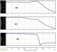
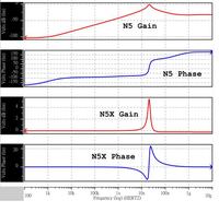
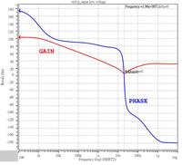
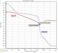
Here are the simulation results for the loop stability checking both for input(N1 and N3) and the output(N5)

For the input:


For the output:


Honestly, I don't know how to interpret these data.
Thanks to the two of you..
 

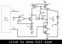
The AC result seems confused. To break the loop, a big inductor (>10GH) can be inserted at N5 and connected at OPb output directly. And inject a AC source (ac=1V) behind the inductor.
Check AC for N5x.
 
Last edited:
  • Like
Reactions: allennlowaton

    V

    Points: 2
    Helpful Answer Positive Rating

    allennlowaton

    Points: 2
    Helpful Answer Positive Rating
hello leo_02.
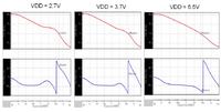
Here is the result of the AC analysis of the circuit diagram you provided.
The output node in the simulation is the OP output.
From Vdd=2.7~5.5V, it's very clear that it's not stable.
 

Hi allennlowaton,

Did you already check the dc operating points (as I have recommended)?
Nevertheless, my question is: Why do you think it is unstable? Sorry, but I cannot read the scale values - neither the magnitude nor the phase.
However, according to one of the diagrams shown earlier in this thread the phase starts for low frequencies with zero deg.
This indicates dc instability (bad resp. no operating point) because for low frequencies you always must have negative feedback! With respect to this requirement - what about your last phase functions (down to 1mHz or so, not starting at 100 Hz) ?
 
  • Like
Reactions: allennlowaton

    V

    Points: 2
    Helpful Answer Positive Rating

    allennlowaton

    Points: 2
    Helpful Answer Positive Rating
Hello dgnani and leo_o2..
Here are the simulation results for the loop stability checking both for input(N1 and N3) and the output(N5)

For the input:


For the output:


Honestly, I don't know how to interpret these data.
Thanks to the two of you..

If you want to follow the simple method I suggested (splitting the the output wire with the AC source w/o the extra devices) then I need to see two plot, magnitude and phase of the loop gain
v(n5_op)/v(n5)
not the two isolated plots w/o phase
All you need for stability is in there

Also as LvW suggested include a lower range of frequencies

You can also try to cut to the chase a insert a capacitor say 1pF between N5 and N1 (to boost negative feedback at high freq) and see if that solve the oscillation
 
Last edited:
  • Like
Reactions: allennlowaton

    V

    Points: 2
    Helpful Answer Positive Rating

    allennlowaton

    Points: 2
    Helpful Answer Positive Rating
If you want to follow the simple method I suggested (splitting the the output wire with the AC source w/o the extra devices) then I need to see two plot, magnitude and phase of the loop gain
v(n5_op)/v(n5)
not the two isolated plots w/o phase
All you need for stability is in there
I tried to follow your suggestion but I found the resulting graphs very confusing. Anyway, as leo_02 suggested I was able to produce this output shown at Reply #26. The red ones are the gains and below it are its corresponding phase. It is unstable since the phase margin are very low.

---------- Post added at 00:34 ---------- Previous post was at 00:33 ----------

If you want to follow the simple method I suggested (splitting the the output wire with the AC source w/o the extra devices) then I need to see two plot, magnitude and phase of the loop gain
v(n5_op)/v(n5)
not the two isolated plots w/o phase
All you need for stability is in there
I tried to follow your suggestion but I found the resulting graphs very confusing. Anyway, as leo_02 suggested I was able to produce this output shown at Reply #26. The red ones are the gains and below it are its corresponding phase. It is unstable since the phase margin are very low.
 

I find it surprising it should be as simple as it comes, I guess I will have to double check it myself but I am under the impression it is a problem of implementation, can you post the SPICE line where you assert the inline AC source and the plot instruction?
 
xop2 vb4 n1 n3 n5x op2stageP

vn5 n5 n5x dc 0v ac 1v

where xop2 is the subcircuit of OP, vb4 = bias voltage, n1 = pos.input, n3=neg.input
 

that looks perfectly correct: what about plotting
v(n5x)/v(n5) in magnitude and phase
Or if it is easier calculate
vdb(n5x)-vdb(n5)
vp(n5x)-vp(n5)
which is the same thing - by vp() I mean the phase of the AC wave

As you can already see in you plots at low frequencies n5x is contributing only around 20MHz and is at 0bB otherwise, when you do the difference of the two waves (which is the ratio of the voltages in dB scale) you will get the opposite (in sign) of n5 almost everywhere except around 20MHz where the contribution of N5x will push the plot to negative -wrong- more positive values
From what I see you should get
a DC gain of 100dB, a -3dB bandwidth of 1kHz and a transition frequency of around 20Mhz
The loop gain will not stay below 0dB but go back up to ~30dB, which is a clear sign of instability - no gain margins
Once you have the point where the loop gain phase crosses 0degree, that should be the frequency of oscillation of your currents
 
Last edited:
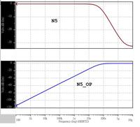
This is the resulting graph for the operation:
vdb(n5x)-vdb(n5) and -1*vp(n5)


---------- Post added at 07:42 ---------- Previous post was at 07:36 ----------

transition frequency of around 20Mhz --- is this the same with unity gain frequency? I really don't get this one..thank you..
 

why -1*vp(n5) instead of vp(n5x)-vp(n5)?

in any case, yes this is correct, n5x does actually push in the opposite direction than I stated before and prevents the loop gain from ever crossing 0dB
As you can see there is still (positive) gain at 0 deg crossing that will be the oscillation frequency of you system (~20MHz)

now you need to make sure that the negative feedback loop, through MP4 (which acts as an inverting amp) to node N1 dominates over the positive feedback loop to N3 through MP5

There are various options more or less elegant:
the simplest one is to add a very large cap to node N3 so this will look like AC ground at high frequency and kill the positive feedback loop

A more elegant way would be to use the miller effect so you can use a smaller cap, I think that putting a cap between N5 and N3 (I said N1 in an earlier post but I think it's wrong) in the 100f-1pF range should do the trick

Regenerate tran and AC analysis in that case and let's see
 
Last edited:
Good day to all of you!!

Regenerate tran and AC analysis in that case and let's see

Hello dgnani:
Shown below are the AC and transient analyses results. A 0.5pF is being added on N5 and N3. The Vdd of this simulation is just from 2.7V to 5.5V(Li-ion batt), the range of my application, instead of previous simulations (Vdd = 0 to 5.5V).


I measured the oscillation frequency of the ringing part of the transient and it's around 2.2MHz.
 
Last edited:

This does not make much sense. At what value of vdd are you running ac analysis?

Let's try the easy way first: forget about the miller cap between node N5 and N3 and add a large cap say 100pF between the non-inverting input of opamp b and ground, this should kill the loop gain at high frequency, if not then we have a different problem...
 
Status
Not open for further replies.

Part and Inventory Search

Welcome to EDABoard.com

Sponsor

Back
Top