Continue to Site

Welcome to EDAboard.com

Welcome to our site! EDAboard.com is an international Electronics Discussion Forum focused on EDA software, circuits, schematics, books, theory, papers, asic, pld, 8051, DSP, Network, RF, Analog Design, PCB, Service Manuals... and a whole lot more! To participate you need to register. Registration is free. Click here to register now.

CMOS Transistor size ratio

Status
Not open for further replies.

erikwikt

Junior Member level 1
Joined
Nov 21, 2010
Messages
18
Helped
0
Reputation
0
Reaction score
0
Trophy points
1,281
Activity points
1,445
Hi
I apologize if this is´t the right forum for this kind of question but i have been searching the forum and have´t been able to find a suitable answer to my problem .

The problem is that I have to size CMOS transistors accordingly to a specific ratio to (under my understanding) get equal rise and fall time.

The design is a four input pseudo-NMOS-gate with the ratio for the NMOS W/L = (1.8/1.2) and for the PMOS W/L = (3.6/1.2) with the foundery of 0.25um.

I just want to be clear that im not looking for the strait up answer to my problem but instead a push in the right direction..

Hope that you understand my description and that you have time to answer.

Best regards Erikwikt.
 

Hi,

Please go through this PDF for better understanding of sizing the transistor.

**broken link removed**
 
  • Like
Reactions: ashwiz and erikwikt

    erikwikt

    Points: 2
    Helpful Answer Positive Rating

    ashwiz

    Points: 2
    Helpful Answer Positive Rating

    rockykumar

    Points: 0
    your link has been broken. Would you mind to share the link again please?
Hi vlsi123, thanks for the quick answer.

I have been reading the PDF that you linked to me and I think its great! But I have a couple of questions in my way of thinking.

In the problem that i descibled it was said that the ratio for the NMOS (as an example) transistor should be (1.8/1.2).
Because of the fact that it has decimal numbers in both over and under the division sign. Can I simplify it to 3/2? So that I get strait lambdas?

To my second question, I have read from other sources that a rule of thumb is that the with of the PMOS should be twice the with of the NMOS because of the mobility in the material.

Now I am using MicroWind as my design program and from the program I can extract the minimum length of the gate for both the NMOS and the PMOS, which is 2 lambda.
So if the with of the PMOS gate has to be 3 times larger then the length, will the total gate with be [(minimum length) * (the mobility rule) * (the with ratio)] = (2 * 2 * 3) = 12 lambda?

Yours ErikWikt
 

... Can I simplify it to 3/2? So that I get strait lambdas?
Sure; that's fine!

To my second question, I have read from other sources that a rule of thumb is that the with of the PMOS should be twice the with of the NMOS because of the mobility in the material.
The actual silicon mobility ratio µn/µp ≈ 2.7 , hence a factor of 2.5 or 3 comes closer to reality.

... the minimum length of the gate for both the NMOS and the PMOS, which is 2 lambda.
So if the width of the PMOS gate has to be 3 times larger then the length, ...
3 times :?: 3/2=1.5 :!:

... will the total gate with be [(minimum length) * (the mobility rule) * (the with ratio)] = (2 * 2 * 3) = 12 lambda?
No: (2 * 3 * 1.5) = .
 
Hi erikl
The size ratio for the NMOS transistor should be 3/2 and 3 (3/1) for the PMOS.
So wont the width for the PMOS be equal to 2 * 3 * 3 = 18 and 2 * (3/2) = 3 (or 6 if i chose the length for the NMOS gate to be 4)?
 
Last edited:

The size ratio for the NMOS transistor should be 3/2 and 3 (3/1) for the PMOS.
So wont the with for the PMOS be equal to 2 * 3 * 3 = 18 and 2 * (3/2) = 3 (or 6 if i chose the length for the NMOS gate to be 4)?

Again: no, sorry! Why:?:

(minimum length) * (the mobility rule) * (the width ratio) = 2 * 3 * 1.5 = 9
In your equation for the PMOS width, (the width ratio) = width ratio of NMOS. The mobility ratio of 3 already takes care :!:

NMOS W/L = 1.5 . For similar electrical behavior of PMOS & NMOS use
W/L(PMOS) = (µn/µp) * W/L(NMOS) ≈ 3*W/L(NMOS)

You don't need to double the PMOS ratio (the doubling at your original source PMOS/NMOS W/L ratio is caused by a mobility ratio assumed to be =2); now we calculate with a mobility ratio=3.

So finally: W/L(NMOS) = 3/2 (or 6/4) and W/L(PMOS) = 9/2 (or 18/4)

Hope I could present this graspably!

BTW: If you design for a mobility ratio of 2 or of 3 depends on your personal feeling: quite a lot of books and papers use a ratio of 2 (hence the PMOS is a bit wispier than the NMOS), it is (somewhat) easier to calculate ;-), and - last not least - it saves costly silicon area. A design ratio of 3, however, is closer to reality, better for NMOS/PMOS symmetry (concerning Ids, gm, fan out ...), achieves (somewhat) faster circuitry - just is (somewhat) more expensive.
So choose up to your requirements - or up to your taste! ;-)
 

Hi again guys. Sorry for the terrible late answer but my studies has been eating me alive....
I just want to thank you guys for the help with my question! =D
It really was a homework if that wasn't clear and I got total points on it as well!

Thanks again for the help!
 

if you just want to get equal rise and fall time,
you can use a capacitor load and tansient analysis,
find the rise and fall time of Vout,
then adjust the W/L of NMOS and PMOS.
usualy,the mobility ratio µn/µp is not equal for different fab process.
but the design theory is the same as what erikl's said.
 

Hello,
In a circuit I have changed PMOS of W from 240nm to W/L=540nm/180nm. I want to know for NMOS how much the W from 240nm has to be changed if the L remains the same i.e.180nm? The circuit is being implemented in Cadence.
 

Just keep the old PMOS/NMOS ratio. If you want to consider the µn/µp ratio (which is about 4.7 for 180nm CMOS), you could adjust the PMOS(W/L) / NMOS(W/L) ratio for this factor.
 

Just keep the old PMOS/NMOS ratio. If you want to consider the µn/µp ratio (which is about 4.7 for 180nm CMOS), you could adjust the PMOS(W/L) / NMOS(W/L) ratio for this factor.

Dear Erikl,
Thanks so much for responding:). Could you explain more in this area as to exactly what should be done? How can I adjust the PMOS(W/L) / NMOS(W/L) ratio by considering the µn/µp ratio?
 

How can I adjust the PMOS(W/L) / NMOS(W/L) ratio by considering the µn/µp ratio?

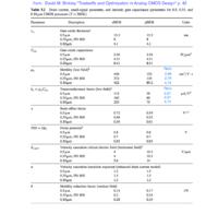
As the mobility ratio for 180nm CMOS bulk processes is about 4.7 (s. the image below), the PMOS(W/L) ratio should be this factor greater than the NMOS(W/L) ratio, if you want the same drive strength from both transistors. So if you selected W/L=540nm/180nm for your PMOS, your NMOS needs only a W/L=115nm/180nm. For more info see e.g. the book named at the image below.

 
As the mobility ratio for 180nm CMOS bulk processes is about 4.7 (s. the image below), the PMOS(W/L) ratio should be this factor greater than the NMOS(W/L) ratio, if you want the same drive strength from both transistors. So if you selected W/L=540nm/180nm for your PMOS, your NMOS needs only a W/L=115nm/180nm. For more info see e.g. the book named at the image below.


Thanks so so much Erikl:-D You are being a gr8 help to me. Really *** is using you to help me out...Amen...*** Bless You...0:)
 

Please consider that all these ratio considerations are just good approximations but not accurate and don't consider effects of layout, temperature and process variation (ss/ff/sf/fs). If you really want a minimal difference between rise/fall times at all corners (for example when creating clock buffers), then you have to numerically optimize the netlist, preferrably an extracted one post-layout.
 

As the mobility ratio for 180nm CMOS bulk processes is about 4.7 (s. the image below), the PMOS(W/L) ratio should be this factor greater than the NMOS(W/L) ratio, if you want the same drive strength from both transistors. So if you selected W/L=540nm/180nm for your PMOS, your NMOS needs only a W/L=115nm/180nm. For more info see e.g. the book named at the image below.


I am designing a 3 input nand gate on microwind( layout level) and on Dsch2-7 (transistor level).

i am given the Nmos sizes: W=4.5 pi L=2.5 pi
with the foundary = CMOS018

I am told to use the same length of PMOS as i used for NMOS. however, i have to find the width of PMOS so that i have equal rise and fall time.

is there a special relationship between width of NMOS and PMOS?? please help out. or direct me to a link.
 

Everything you need is described above in this thread: read it attentively :)

I have a comment, though, on the page you show as an image from David Binkely's book. The values for carrier mobility are strange. Both UMC 0.18u and TSMC 0.18u have a carrier mobilty ratio of approx 2.6, not 4.7 as in Binkley's table.

Slainte!
H
 

... David Binkely's book. The values for carrier mobility are strange. Both UMC 0.18u and TSMC 0.18u have a carrier mobilty ratio of approx 2.6, not 4.7 as in Binkley's table.

Strange, yes. May be an anomaly of his special process? Rather bad PMOSFETs?
Our 0.18 processes (from 2 other foundries) also showed µ ratios in the vicinity of 2.3 .. 2.5 .

Slainte!
H
Irish or Scottish, Hans? ;-)
 
Last edited:

Strange, yes. May be an anomaly of his special process? Rather bad PMOSFETs?
Our 0.18 processes (from 2 other foundries) also showed µ ratios in the vicinity of 2.3 .. 2.5 .

Since the µ depend on doping, and customers of foundries normally want to use similar designs when going to a smaller technology node, I can scarcely imagine what could bring a foundry to doing this 4.7 ratio ... they'd have to do it on purpose, but for what purpose?

Irish or Scottish, Hans? ;-)

Scottish ... I studied English in Edinburgh, a long time ago :)
 

Sir have you parameters value related to 22nm technology??

and value for voltage suply for this 22nm technology??


thanking you...

- - - Updated - - -

Sir I am not able to download this pdf is there any other pdf like this available??

- - - Updated - - -

value of lambda would be???
 

Status
Not open for further replies.

Part and Inventory Search

Welcome to EDABoard.com

Sponsor

Back
Top