Continue to Site

Welcome to EDAboard.com

Welcome to our site! EDAboard.com is an international Electronics Discussion Forum focused on EDA software, circuits, schematics, books, theory, papers, asic, pld, 8051, DSP, Network, RF, Analog Design, PCB, Service Manuals... and a whole lot more! To participate you need to register. Registration is free. Click here to register now.

Matching the biasing circuit to the core amplifier

Status
Not open for further replies.

Junus2012

Advanced Member level 5
Joined
Jan 9, 2012
Messages
1,552
Helped
47
Reputation
98
Reaction score
53
Trophy points
1,328
Location
Italy
Activity points
15,235
Hello friends,

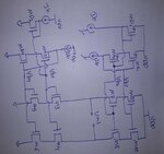
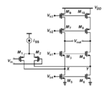
below is an example of folded cascode ampliifer,

you see transistors M2-to-M10, these transistors are biased with VB1-to-VB4.
folded.PNG

While VB1 and VB2 is a biasing voltage for the cascode transistors M3,M4,M7 and M8 and it is not critical, but Vb3 and VB4 are biasing the upper and down mirror, if the transistors generating these voltages are not matched to the transistor in the ampliifer this will lead to mismatching in the current.

My question, when you design such circuit, do you consider to match the biasing circuit to the core circuit,

I have searched in many literature and I usually see them seperating both, I am not sure how they are matching it

Thank you very much
Best Regards
 

These are current sources rather than mirrors. A current reference and mirror circuit is usually generating the bias levels.
 
These are current sources rather than mirrors. A current reference and mirror circuit is usually generating the bias levels.

Hello Fvm,
Thank you for your reply and for your correction,
yes I mean the current source....as you said I usually generate these biasing voltages using current reference and mirror.... and here exactly my question, the mirror is shown in the circuit above as it is supposed to be part of the biasing circuit, any way, do I need to match these mirror to these current sources ? In my opinion it should be, but I am not sure

Hope I made the issue more clear

- - - Updated - - -

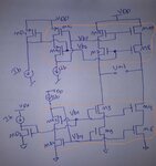
I attached you below the circuit with the biasing mirror so we can discuss on it

New Doc 19.jpg

Do I nead to match MX1 to M9&M10, Mx2 to M7&M8
MX3 to M3&M4 , MX4 to M5&M6

If yes it means I have to consider them together when I make the common centroid plan

What about if other part in the chip are using the same baising voltage of VB1-VB3, including them alltogether in the same matching array will make it complicated
 

Hello FvM

I found this layout for another folded circuit, you see here he matched M5 to M6 but not to the biasing voltage Vb1 !!

fooolded.PNG
 

A simple think to do is to include inside the amplifier the complete mirror for biasing you amplifier current sources. Then distribute currents from outside going to the amplifier mirrors. This way you know you have to match transistors that are physically close and not on opposite ends of the chip.
 
A simple think to do is to include inside the amplifier the complete mirror for biasing you amplifier current sources. Then distribute currents from outside going to the amplifier mirrors. This way you know you have to match transistors that are physically close and not on opposite ends of the chip.

Dear Suta,

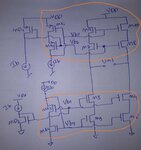
If I understood you write, are you suggesting the scheme in my post #3, shown below as well, I have grouped the transistors to be matched

folo.jpg

Thank you
 

Thank you Suta,

so it is ok to sacrifice some power consumption for the sake of matching,

I am thinking that these mirrors will carry for example 1/4 of the required current, means in the above circuit transistors MX1-Mx4 carry 1/4 of the required current in M5-M10, although I have read somewhere that best matching when mirror ratio is one.

According to your confirmation, if I need Vb1-Vb4 in another part of the chip then a separate biasing mirror should be supplied and matched there separately.


Could you please tell me why in most if not all IEEE papers, they dont show this scheme, thus they count less number of transistors and less power as well.

Deasign without matching consideration will be Ok for schematic simulation but with layout and Montecarlo simulation it mostly fails due to large mismatching
 

You have current sources in the amplifier. These need to be biased somehow. Best is with mirrors and mirrors need current to operate. You have to put some consumption there.
At a chip level we distribute currents, not voltages, well, most of the time. So yes, if you need to bias something that's somewhere else, in a different block, then you just build a mirror there.
Mirrors in this aspect are something given and not really of interest. Papers, I gues concentrate on amplifier design adn don't really focus on the infrastructure around them. Just a guess.
 
@Junus2012
sutapanaki is correct. The picture from you first post is from Razavi. While M3-M4 and M7-M8 serve as casodes, let's say they can be biased with more or less controlled voltage. However, M5-M6 and M9-M10 are current sources and if you want to control the current in them you bias them using current mirrors, for example, as you drew it in your picture.
See Baker (https://cmosedu.com/cmos1/book.htm), he always control currents in branches.

Regarding IEEE papers, sometimes there is shown more or less. As sutapanaki metioned, very often authors want to concentrate on the core circuit.
 
Thank you friends,

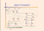
I have also seen this slide, he is matchiung the current mirror from the biasing circuit to the ampliifer core

Which follow your suggestion,

maaaa.JPG

- - - Updated - - -

you see how he groubed the matchede transistors

- - - Updated - - -

@Junus2012
sutapanaki is correct. The picture from you first post is from Razavi. While M3-M4 and M7-M8 serve as casodes, let's say they can be biased with more or less controlled voltage. However, M5-M6 and M9-M10 are current sources and if you want to control the current in them you bias them using current mirrors, for example, as you drew it in your picture.
See Baker (https://cmosedu.com/cmos1/book.htm), he always control currents in branches.

Regarding IEEE papers, sometimes there is shown more or less. As sutapanaki metioned, very often authors want to concentrate on the core circuit.

Thank you t4_V for your reply

Indeed Baker always design biasing circuit seperated from core amplifier and upto my weak knowledge he never gave an example to consider matching them, if you know in which circuit then please refer me to the page or to that chapter
 

Yes, very good slide.

Regarding Baker, he always writes or it is on pictures that PMOS and NMOS are identical and some of them are just multiplication (so also matched). The same as here:

opamp.png

Source: https://payhip.com/b/5Srt ("Preview" button in top right corner)

"All the other NMOS transistors are identical. The same is true for PMOS devices." Just M3 is doubled to have twice the current that M8.

Generally, matching is extremely important in analog IC design. In that way you control currents and voltages in a circuit.

=====

I do not believe. Somebody put Baker in Google Drive: **broken link removed** . See page 1.100:
PMOS are 100/2
NMOS are 50/2

Other dimensions are shown in the picture.
 
Last edited:

While VB1 and VB2 is a biasing voltage for the cascode transistors M3,M4,M7 and M8 and it is not critical, but Vb3 and VB4 are biasing the upper and down mirror, if the transistors generating these voltages are not matched to the transistor in the ampliifer this will lead to mismatching in the current.

My question, when you design such circuit, do you consider to match the biasing circuit to the core circuit,

If Id{M9}!=Iss/2 + Id{M5}, then your output common mode will either end up in either Vdd or gnd. Isn't this why you would need a common mode feedback circuit to make sure that does not happen? What am I missing here?

- - - Updated - - -

Thank you friends,

I have also seen this slide, he is matchiung the current mirror from the biasing circuit to the ampliifer core

Which follow your suggestion,

View attachment 159194

This is completely different from the circuit the OP has posted. This has a single ended output.
 

Regarding Baker, he always writes or it is on pictures that PMOS and NMOS are identical and some of them are just multiplication (so also matched).

Source: https://payhip.com/b/5Srt ("Preview" button in top right corner)

"All the other NMOS transistors are identical. The same is true for PMOS devices." Just M3 is doubled to have twice the current that M8.

Generally, matching is extremely important in analog IC design. In that way you control currents and voltages in a circuit.

=====

I do not believe. Somebody put Baker in Google Drive: **broken link removed** . See page 1.100:
PMOS are 100/2
NMOS are 50/2

Other dimensions are shown in the picture.

Hello T4,

Thank you for your nice explanation

yes I believe that matching is important for layout, no doubt about it, but I think you are referring to another kind of matching in your explanation

- - - Updated - - -

****************************************************

Dear Vivekroy,

my first post is not a complete circuit, nor the single ended last one, I just presented it to see if I need to match the biasing mirror to the core amplfier at the time of layout design,
 

yes I believe that matching is important for layout, no doubt about it, but I think you are referring to another kind of matching in your explanation

What exactly matching do you think of? How can I help you?
In your original Razavi folded cascode opamp following are cricital and must be matched:
- M1-M2
- M5-M6 with other diode-connected NMOS that provides bias voltage and hence set the desired currents in M5 and M6
- M9-M10 with other diode-connected PMOS that provides bias voltage and hence set the desired currents in M9 and M10

M3-M4 and M7-M8 are cascodes so you do not set currents in them by Vb1, Vb2. Currents are set by M5-M6 and M9-M10, respectively.

Dear T4_V

Thank you very much for your wish to help me, I do appreciate it

Please refer to the circuit bellow,

Anyway, Mr. Suta also confirmed it, and I am going to match the grouped transistors, means biasing mirror has to be matched in the same matching array of the core amplifier transistors,
Also as Suta mentioned, we can supply the current of these mirrors by means of copy of the reference current in the circuit

Thank you once again

mate.jpg
 

Dear T4_V
Anyway, Mr. Suta also confirmed it, and I am going to match the grouped transistors, means biasing mirror has to be matched in the same matching array of the core amplifier transistors,
Also as Suta mentioned, we can supply the current of these mirrors by means of copy of the reference current in the circuit
View attachment 159232

Yes, exactly. You want to match:
- PMOS Mx1, M9, M10
- PMOS Mx2, M7, M8
- NMOS Mx3, M3, M4
- NMOS Mx4, M5, M6

Even if core and bias circuits are in separate blocks, one should think of them as unity.
 
Yes, exactly. You want to match:
- PMOS Mx1, M9, M10
- PMOS Mx2, M7, M8
- NMOS Mx3, M3, M4
- NMOS Mx4, M5, M6

Even if core and bias circuits are in separate blocks, one should think of them as unity.

Thank you Suta and T4,

That is the answer I was looking for,
at the start I was designing the biasing circuit separately from the core, but after your help I copied the current from the biasing circuit and created a new mirror by Mx1 to Mx4 to layout with the core amplifier
 

Hello all

I just wanted to share this matching plan from the famous book "The afrt of analog layout", it is clearly mentioned in his plan to include the biasing transistors with the core amplifier

Thank you for your help in this post

meao.JPG
 
  • Like
Reactions: t4_v

    t4_v

    Points: 2
    Helpful Answer Positive Rating
Yes it is up to designer, team leader so on whether to include bias in the same or separate block.
 
Status
Not open for further replies.

Part and Inventory Search

Welcome to EDABoard.com

Sponsor

Back
Top