OZZAA
Member level 1

- Joined
- Feb 10, 2020
- Messages
- 33
- Helped
- 0
- Reputation
- 0
- Reaction score
- 0
- Trophy points
- 6
- Activity points
- 325
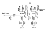
I already designed Class AB power amplifier (Cascode CMOS TSMC 180nm - 5GHz), and after I choosed Load and Source impedances from source and load pull simulations according to getting max. PAE.
I designed the in and out matchig circuits according to these values.

When I tested the S-parameter using LSSP at ADS Keysight (input power = 5dBm).
S11 and S22 are high values.


when I modified the matching circuits to decrease S11 and S22 the PAE values goes lower as well (However the gain is increased !!!:thinker .
.


I do not know where is the problem in this design.
Thanks in advance
I designed the in and out matchig circuits according to these values.

When I tested the S-parameter using LSSP at ADS Keysight (input power = 5dBm).
S11 and S22 are high values.


when I modified the matching circuits to decrease S11 and S22 the PAE values goes lower as well (However the gain is increased !!!:thinker


I do not know where is the problem in this design.
Thanks in advance


