Continue to Site

Welcome to EDAboard.com

Welcome to our site! EDAboard.com is an international Electronics Discussion Forum focused on EDA software, circuits, schematics, books, theory, papers, asic, pld, 8051, DSP, Network, RF, Analog Design, PCB, Service Manuals... and a whole lot more! To participate you need to register. Registration is free. Click here to register now.

Sooch current mirror

Status
Not open for further replies.

Junus2012

Advanced Member level 5
Joined
Jan 9, 2012
Messages
1,552
Helped
47
Reputation
98
Reaction score
53
Trophy points
1,328
Location
Italy
Activity points
15,235
Dear friends

In my most circuits I use the wide swing current mirror for biasing my amplifier and most desingers use it specially for low voltage aplication.
However there is comparable mirror performance named the "Sooch current mirror" which I attached its image.

It is known that this circuit consume more headroom voltage at the input making it unapplicable for low voltage circuits, but from my hand calculation I still see that this circuit fine with 3.3 V CMOS technology which I am using so why this circuit is not common in this technology or above.

is there any other drawback that makes the wide swing mirror more preferable over it ?
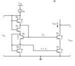
sooch.PNG

Thank you very much
 

I don't have experience with it, but think about these:
a, Hand calculations are not so effective, they won't tell you how it handles process/supply/temperature variation. Run simulation.
b, How the top current source is implemented (should use cascode device, how that device handle process/supply/temperature variation)?
c, And how about the area of above circuit, if bigger then does it mean that it is more unsensitive to mismatch? If not probably that is the main reason why not to use.
 
Dear frankrose,

Thank you for your reply

That was my inquiry indeed, still good analog designers like you are not preffering or not try this circuit,

I have tried the circuit by simulation and still giving good results,
for the upper current source I connectede wide swing mirror to provide the current

if we compare this circuit when it is working with the 3.3 V then it seems better than the wide swing mirror counterpart as the latter one needs an additional branch current to supply the biasing diode transistor
 

if we compare this circuit when it is working with the 3.3 V then it seems better than the wide swing mirror counterpart as the latter one needs an additional branch current to supply the biasing diode transistor
That current is negligible I think, you should find another reason(s). Area, cost, linearity, operation range, mismatch, maybe share these results with true comparison.

for the upper current source I connectede wide swing mirror to provide the current
Why not used another sooch current mirror from PMOS to compare?

You know analog designers regurarly doesn't like when any transistor operates in triode region, especially when they are in a reference branch. M5 of above figure is tipically this case.
 
Thank you frank again

No problem, I wil try to simulate it with a current source provided by PMOS current sooch,

Regarding the M5 as it is working in the triode region, even the wide swing mirror if you biase it with stack transistor then also that biasing transistor will be in the triode region,,, I think it should not be a problem as Behzad Rezavi proved that stack transistors match better to the circuit.

You told me to ignore the additional current source from my comparesion, actually the additional current source add more complixity to the mirror circuit that is providing it as it will have more branches,
 

Regarding the M5 as it is working in the triode region, even the wide swing mirror if you biase it with stack transistor then also that biasing transistor will be in the triode region,
This is not really true. When I designed high swing mirror none of the transistors were in triode region, over PVT corners. I didn't use stacked diodes to bias cascode transistors. Point of this wide swing mirror is the single diode connected device which bias the cascode transistors. With stacked transistors the matching is the best but it won't be high swing.

You told me to ignore the additional current source from my comparesion, actually the additional current source add more complixity to the mirror circuit that is providing it as it will have more branches,
Nope, I didn't tell. At least here I didn't. And it is not complex becasue of an extra branch. Think about it, ICs are filled with 10s,100s,1000s of current mirrors! Complexity for me rather to use a non MOS device, or a MOS in triode region...or clock. Not an extra mirror.
 
Perhaps this mirror is ok with 3.3v supply. At the diode side you have 2Vgs from gnd up and this reduces the compliance voltage for the P current source. This can be a problem in technologies that work at 1V or maybe even 1.8V. That being said, I have not used this kind of mirror.
 
Thank you Suta for being active on my post,

Allen Holberg use this circuit but instead he put resistor rather than M5 and M6.

Dear Frank, you braught me back to one of my former post regarding the stack transistor performance comparing to single diode transistor, I think at the time also Suta was defending the stack connection, I would like to make this topic again active with you,
See the image below and please tell me your opinion, which one is better for (A or B or C) you and why ?

New Doc 64.jpg

Many thanks
 

Yes, that current mirror with resistors I have used before. The cascode voltage is then Vgs+IR. However, I still think that the version with the stack transistors should track better.
 
Yes, that current mirror with resistors I have used before. The cascode voltage is then Vgs+IR. However, I still think that the version with the stack transistors should track better.

Yes Suta and Holberg refer to it as self biased cascode mirror, I also attached it here

sooch_holberg.PNG

Concerning thee stack transistor, as I learned from in the former post it the stack one should be better, This is also stated by Jakon and Razvi.. They argued to use same channel length for better matching,

but to be ohnest, I don't know why then one use the connection (C) from my image... it uses the same L of the matched mirror

Thank you again
 

I don't think you should stick to using the same size transistors in the stack as they are in the cascodes of the mirror. In your figure B both cascodes and stacked transistors are 120/1. While it is preferable to have the same L=1u for both, W can be different and it should be. You are trying to build a voltage by the stack that is higher than Vgs of a single transistor, so you need weaker transistors there, hence smaller W. At the same time you don't really want to go to the minimum for the technology W in the stack. This way you end up using resonable W and stack few transistors.
 
Yes Suta and Holberg refer to it as self biased cascode mirror, I also attached it here

View attachment 155217

I tried this circuit once in 28nm. The issue I faced was that the resistor variation was too much for my application. Extreme corners of MOS needs to be combined with the extreme corner of resistor (it is debatable whether we need to be so pessimistic) but that gave me issues.

@Junus2012, the current mirror that you have shared is very similar to a low voltage cascode current mirror. The only advantage I can see is that it requires one reference current lesser than the low voltage one. The low voltage cascode current mirror requires another arm of stacked transistors supplied by a reference current source to generate the the bias voltage of the cascode transistor.
 

I don't think you should stick to using the same size transistors in the stack as they are in the cascodes of the mirror. In your figure B both cascodes and stacked transistors are 120/1. While it is preferable to have the same L=1u for both, W can be different and it should be. You are trying to build a voltage by the stack that is higher than Vgs of a single transistor, so you need weaker transistors there, hence smaller W. At the same time you don't really want to go to the minimum for the technology W in the stack. This way you end up using resonable W and stack few transistors.

Dear Suta,

I got your point, and actually I followed that in my design, just like in this picture

cas.jpg

- - - Updated - - -

I tried this circuit once in 28nm. The issue I faced was that the resistor variation was too much for my application. Extreme corners of MOS needs to be combined with the extreme corner of resistor (it is debatable whether we need to be so pessimistic) but that gave me issues.

@Junus2012, the current mirror that you have shared is very similar to a low voltage cascode current mirror. The only advantage I can see is that it requires one reference current lesser than the low voltage one. The low voltage cascode current mirror requires another arm of stacked transistors supplied by a reference current source to generate the the bias voltage of the cascode transistor.

Dear Vivekroy,
Nice to hear from you again,

Actually I don't prefer to use the one with resistor, because the resistor can vary by 25 % with process corner and temperature, rather I prefer the one in my first post.
As you said it has less branch less, it means less power dissipation and the same performance of wide swing mirror.. the only limitation is the minimum input voltage required for this circuit is bigger making it not suitable for small technology, Gregorian was telling that this circuit is suitable for technology voltage above 3 V.

if you catch my question from the start, I was wandering why even people working with 3.3 are still not using it commonly ?
 

Actually, even the mirror with the stacked transistors can work with a single input current but it needs a small start-up circuit and it can be done without consuming extra.
 
Actually, even the mirror with the stacked transistors can work with a single input current but it needs a small start-up circuit and it can be done without consuming extra.

Dear Suta,

This is new idea to me, can you please refer me to some written work to read about it
 

if you catch my question from the start, I was wandering why even people working with 3.3 are still not using it commonly ?

I can't speak for other designers but whenever I had some extra voltage headroom, I used to use it in the reference current sources. The bias current typically comes from a bandgap and it needs to be quiet accurate. By increasing the over-drive for the same current, I decrease the gm and thus I get lesser mismatch. In my applications, the bandgap needed to generate anything between 20-40 reference currents. A bit of area saving there goes a long way in reducing the overall area. The penalty is an extra reference for some blocks (thankfully not all blocks required it).
 
Thank you friends for your nice contribution
 

Status
Not open for further replies.

Part and Inventory Search

Welcome to EDABoard.com

Sponsor

Back
Top