Continue to Site

Welcome to EDAboard.com

Welcome to our site! EDAboard.com is an international Electronics Discussion Forum focused on EDA software, circuits, schematics, books, theory, papers, asic, pld, 8051, DSP, Network, RF, Analog Design, PCB, Service Manuals... and a whole lot more! To participate you need to register. Registration is free. Click here to register now.

Gyrator implementation of chip inductor

Status
Not open for further replies.
You can observe this on figures you have plotted.

Your gm is constant in green line.


I explained it several times. If you want to have constant and linear Gm for you structure you should use source degeneration.

gm3.png

Don't misunderstand me but I suggest you to read CMOS theory before designing these kind of circuits, it will help you a lot.
 

Thanks for your advice.

For https://github.com/promach/frequency_trap , I am having problem getting the right AC analysis plot.

Therefore, I went back to Gm2 calculation. I have the following plot, should I use rms value ? Besides, did I do anything wrong elsewhere which I had not noticed yet ?

Screenshot from 2017-08-04 11-26-40.png


Yes, the above screenshot is from transient simulation. I am using transient simulation to calculate value of Gm2 because I am not getting the desired AC analysis plot.
 

Try to build the whole circuit.

It is hard to do half of it and gm here also depends on frequency.

I cannot explain here, if you want to find gm. You may add a capacitor at the output, and measure the current and then divide it by input AC voltage that would be your gm value.

But you have to know the output capacitance load which is the input capacitance of upper inverted amplifier.

acgm.png
 

I have already done Gm1, Gm2 all together in the github repo. The screenshot I posted just shown Gm2 circuit block.

1) input capacitance of upper inverted amplifier ? How am I going to determine this ?

2) Why use capacitor C2 at the output for Gm2 value calculation ?
 

L1.png

l2.png

I did not use CL since transistor input has self capacitance but you may add in order to get different values for Leq.

This Leq has self resonance with parasitic capacitors as you see it occurs at 6 GHz so you have to be away from self resonance as much as you can.

Many things happen here but I did a rough simulation and swept R.

As you see in 2.5 GHz i get different L values.

But here my circuit it is suitable to operate at 2.5 otherwise Real part gets high or negative.

Probably it is narrow-band L. I don't have that much experience with active inductors since they are kind of useless because of their high noise.

I wont be able to help you more than this. Good luck.
 

How does the present discussion of Gyrator GHz frequency range relate to the original harmonic trap problem with a center frequency of maximal 100 MHz (1* and 2* PLL fref)?
 

To other ngsice users:

I am simulating active inductor in https://github.com/promach/frequency_trap

Why Vtest = -2 ?

View attachment 140455

I guess when you put inverter it acts like digital gate and it saturates so your output becomes VDD or GND.

We know that inverter can operate as amplifier (If we bias it in VDD/2 so it will have small signal gain) maybe instead of that you can put another gm cell.

- - - Updated - - -

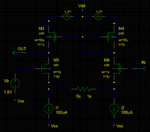
you may set up this circuit.

Second GM is negative Be careful !


gm6.png

gm7.png

Leq=2.5 nH
R= almost zero

Perfect high Q inductor :thumbsup::thumbsup:


BUT !
:-:)-(


As I mentioned previously, this circuit does not have any parasitics so you are not observing self resonance but in real world you wont have these perfect results
 
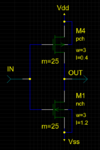
when I put inverter, it acts like digital gate and it saturates.

WHY ? I have made a CMOS inverter with the right W/L ratio

Screenshot from 2017-08-12 18-28-51.png
 

WHY ? I have made a CMOS inverter with the right W/L ratio

View attachment 140481

That is right. show me your GM block too.

Instead of tran simulation, set up S-parameter simulation. you are measuring impedance !!

How you measure your impedance with transient analysis ? you have to find phase difference between input current voltage in order to see the imaginary part ! :roll::roll: That is hard ! Dont forget you are measuring L and R not only R.


100% you have biasing problem here. you have to see the Dc operation points of your circuit before any other simulation
 

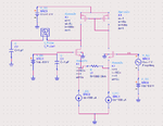
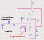
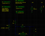
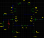
The first schematics is Gm2 block. The second schematics is the top-level.

Screenshot from 2017-08-12 23-13-41.png Screenshot from 2017-08-12 23-15-39.png

Let me do DC analysis first.

Regarding imaginary component and S-parameter, I guess I need some time to learn about simulating them.
 

The first schematics is Gm2 block. The second schematics is the top-level.

View attachment 140484 View attachment 140485

Let me do DC analysis first.

Regarding imaginary component and S-parameter, I guess I need some time to learn about simulating them.

Remember that:

1) Never start other simulations unless you become sure about DC bias.
2) When you measure impedance you better use s-parameter simulation and check Zin.

- - - Updated - - -

I found your problem.

Cc.png

You have to understand the working principle of amplifiers and OTAs deeply.

In AC analysis the gate of M5 should be grounded not Vb. It means that you should put a coupling capacitor.

- - - Updated - - -

- - - Updated - - -


I showed it before but it seems that you are paying attention !
 

In AC analysis the gate of M5 should be grounded not Vb. It means that you should put a coupling capacitor.

Not necessary. DC voltage sources (V_DC) have zero DC & ac impedances.
 

Strange, when I do .OP analysis, I have

Doing analysis at TEMP = 25.000000 and TNOM = 27.000000

Warning: vtest: no DC value, transient time 0 value used


No. of Data Rows : 1

We are using different schematics capture and simulation tools.
Should I resimulate in easyeda online simulator so that we all could edit and debug ?
 
Last edited:

Yeah I think you are right. For simulation it is not necessary.

But I am sure that circuit has biasing problem.


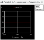
I used Berkeley BSIMv3.3 model, but still some non-sense AC plot. I have zero horizontal line plot at AC amplitude of 0V for V(2) , which is the node above Cs

Screenshot from 2017-08-18 14-57-28.png

I think I need to debug even further what else is wrong, especially mosfet sizing in Gm2 circuit block.

By the way, how do you intepret .op verbose output such as following:

ngspice 703 -> op
Doing analysis at TEMP = 25.000000 and TNOM = 27.000000

Warning: vtest: no DC value, transient time 0 value used

No. of Data Rows : 1
ngspice 704 -> print all
v(1) = 2.900000e+00
v(2) = -1.00000e-01
v.xu2.vb#branch = 0.000000e+00
vc = 2.368405e+00
vd#branch = -2.08230e-03
vdc#branch = 0.000000e+00
vdd = 3.000000e+00
vs#branch = 2.082300e-03
vss = 0.000000e+00
vtest#branch = 0.000000e+00
vx = 1.814641e+00
xu2.1 = 2.750664e+00
xu2.3 = 1.370506e+00
xu2.4 = 1.800000e+00
xu2.5 = 1.585891e+00
ngspice 705 ->
 

Status
Not open for further replies.

Part and Inventory Search

Welcome to EDABoard.com

Sponsor

Back
Top