Continue to Site

Welcome to EDAboard.com

Welcome to our site! EDAboard.com is an international Electronics Discussion Forum focused on EDA software, circuits, schematics, books, theory, papers, asic, pld, 8051, DSP, Network, RF, Analog Design, PCB, Service Manuals... and a whole lot more! To participate you need to register. Registration is free. Click here to register now.

Guard ring connection for nmos in a triple well process

Status
Not open for further replies.

dreamyboy_999

Member level 2
Member level 2
Joined
Mar 1, 2014
Messages
47
Helped
0
Reputation
0
Reaction score
0
Trophy points
6
Activity points
414
I assume in a triple well process, you can have isolated nmos devices by first creating an nwell and then creating the Pwell substrate inside the nwell. My question is: Where should the guard ring (which is an N+ ring connected to the surrounding nwell) connected? Does that need to be connected to the Pwell (body of the inside nmos transistor) or any other potential? (Vss or Vdd).
 

Generally you share the nwell with pmos device and then you connect the ring to VDD.


3p.png

3p2.png
 
Generally you share the nwell with pmos device and then you connect the ring to VDD.


View attachment 132443

View attachment 132444

I am looking at one of the examples provided by the foundry which is an LNA. There are two NMOS transistors in a cascode configuration. The body of the both NMOS transistors is connected to its source (not ground). When I look into the layout, I noticed that the guard ring of both NMOS devices is connected to the nmos p-substrate (not to vdd or anything...) how is that?
 

I am looking at one of the examples provided by the foundry which is an LNA. There are two NMOS transistors in a cascode configuration. The body of the both NMOS transistors is connected to its source (not ground). When I look into the layout, I noticed that the guard ring of both NMOS devices is connected to the nmos p-substrate (not to vdd or anything...) how is that?
.

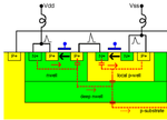
In RF transistors there are 2 gaurds. One is connected to pwell which is yellow in the figure above and it should be connected to source of nmos (body and source are connected to obtain low vt and high linearity). and the other one is connected to nwell which is green and its isolation so you dont need to connect it anywhere unless u share it with pmos and connect it to vdd.

So the ring does not need to be connected to the body of the nmos which is formed inside the nwell? I dunno why they have done that in the layout of the LNA...
 

why do you connect the n-well ring to body ? you make n-well for isolation between psub and p-well. you connect p-well ring to body.

If you have pmos you will share the n-well with pmos using deep n-well and connect the ring of n-well to VDD.
 

why do you connect the n-well ring to body ? you make n-well for isolation between psub and p-well. you connect p-well ring to body.

If you have pmos you will share the n-well with pmos using deep n-well and connect the ring of n-well to VDD.

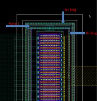
would u please take a look at the attached picture? this is the rf_nmos used in the LNA example provided by the foundry, I can see the P+ and N+ ring connected together through M1..I assume the P+ ring provides a connection to the substrate of the nmos...Please correct me if I am wrong.


I think it is pmos ? are you sure ?

If you check RF transistors they have 6 pins

G D S B NW PSUB

NWELL ring should connect to VDD.

In schematic we connect NWELL to VDD and PSUB to ground

I do not know why they connect NWELL to PWELL !!!!!!! ??
 
Last edited:

If you are after minimum supply induced noise in a (say)
RF amplifier, you might connect the deep NWell to substrate
potential, and the PWell's guardring or tap as well. This will
give multiple layers of Vss-referred capacitance with no real
supply coupling path. If you tie DNW to VDD and PWell to
VSS then you have a large-ish coupling cap to the PWell
that can inject supply noise, with only the stiffness of the
PWell tie to shunt it. PWell movement relative to "prime GND"
modulates the channel via body effect (acting with about
a 0.6 scale factor, like applied gate signal).

Try drawing out the layers and superimposing their parasitic
caps, and then pencil in some noise "aggressors" like VDD(int).
Maybe this will give you a gut understanding.
 
I think it is pmos ? are you sure ?

If you check RF transistors they have 6 pins

G D S B NW PSUB

NWELL ring should connect to VDD.

In schematic we connect NWELL to VDD and PSUB to ground

I do not know why they connect NWELL to PWELL !!!!!!! ??

That is an nmos......That's what I was talking about....

- - - Updated - - -

If you are after minimum supply induced noise in a (say)
RF amplifier, you might connect the deep NWell to substrate
potential, and the PWell's guardring or tap as well. This will
give multiple layers of Vss-referred capacitance with no real
supply coupling path. If you tie DNW to VDD and PWell to
VSS then you have a large-ish coupling cap to the PWell
that can inject supply noise, with only the stiffness of the
PWell tie to shunt it. PWell movement relative to "prime GND"
modulates the channel via body effect (acting with about
a 0.6 scale factor, like applied gate signal).

Try drawing out the layers and superimposing their parasitic
caps, and then pencil in some noise "aggressors" like VDD(int).
Maybe this will give you a gut understanding.

Please correct me if I got it wrong: To put it in a nutshell, it is a good design practice to connect the deep Nwell (N+ ring), and the included Pwell together (as shown in the picture that I attached in the previous msg)? How about the substrate that all of these wells are built in? should I tie it to Vss?
 

Please correct me if I got it wrong: To put it in a nutshell, it is a good design practice to connect the deep Nwell (N+ ring), and the included Pwell together (as shown in the picture that I attached in the previous msg)? How about the substrate that all of these wells are built in? should I tie it to Vss?

You might elect to tie each of the regions together, or separately,
to the signal return / reference (ground). The substrate "handle",
you probably have not much choice regarding; it must be (in JI
standard CMOS and derivatives) the most negative circuit potential.
The NWell as a noise-guard might wants its own "star" style tie (to
ensure that current noise in the net is minimum) or it might like to
be tied directly to the close-in VSS - this depends on what you
think is going on in the neighborhood, and in an IC development
project might be one of the layout what-ifs exercised.

Thank you for your comprehensive answer. Just to make sure I am clear about this::::
" You might elect to tie each of the regions together, or separately, to the signal return / reference (ground) "
So can I basically connect the N+ ring and P+ ring together and connect it to ground? I know you are saying this is not a must (it is a choice). I just want to make sure I am understanding it the right way :)
 

Yes, this is an option (and in some cases the best - but that
is on you to determine).
 
Status
Not open for further replies.

Part and Inventory Search

Welcome to EDABoard.com

Sponsor

Back
Top