Continue to Site

Welcome to EDAboard.com

Welcome to our site! EDAboard.com is an international Electronics Discussion Forum focused on EDA software, circuits, schematics, books, theory, papers, asic, pld, 8051, DSP, Network, RF, Analog Design, PCB, Service Manuals... and a whole lot more! To participate you need to register. Registration is free. Click here to register now.

Low Dropout Regulator Power Supply Rejection

Status
Not open for further replies.

Shady Ahmed

Member level 5
Member level 5
Joined
Jan 26, 2013
Messages
86
Helped
2
Reputation
4
Reaction score
2
Trophy points
1,288
Activity points
2,042
Hi all,

I am designing a low drop out regulator, with the specifications of power supply rejection of -30 dB up to 10 MHz, with load current 2mA.
Using 0.13um technology and 1.8v Supply.
With 1V reference voltage generated from a NON IDEAL band gap circuit & using a NON IDEAL op amp. And the regulated voltage = 1.5v

Here is my schematic:
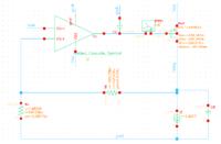


My problem is that I don't understand the factors affecting the power supply rejection.
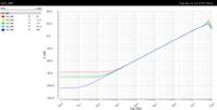
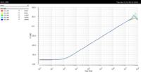
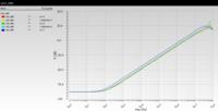
It starts at -60dB at DC, However it keeps increasing and exceeds 0 dB at the KHz range!!

Here are 3 different graphs showing the PSR plots against 3 factors showing that it almost doesn't depend on any of them!

1- PSR against width of the pass transistor


2- PSR against the resistors value


3- PSR against the op amp load capacitance


Thanks for you time, and ur input is much appreciated.
 

PMOS LDOs always have a hard time with HF PSRR, any
groundward jerk on the pass FET gate is directly amplified
(common source amplifier). In normal CMOS techologies
ground parasitics are pervasive. You may need to look at
compensation schemes (like, Miller makes it worse as any
drain jerk - which would include + supply movement,
relative to the fixed Vout - is a gate input stimulus; shunt
comp to VIN is less area efficient but better for HF PSRR,
attenuating rather than amplifying dVIN).

Depending on your available resources, an NMOS "ULDO"
design (using an auxiliary higher voltage supply for the
regulation core, and a lower raw supply at VIN to make
VOUT at very low drop) can be much superior for HF PSRR,
making it only about the error amp response and taking
the more-capacitive pass FET out of the picture pretty
much.

- - - Updated - - -

I note that your comp cap is connected exactly wrong
for HF PSRR - return C4.minus to VIN, not gnd!, and
observe.
 
Hi all,

I am designing a low drop out regulator, with the specifications of power supply rejection of -30 dB up to 10 MHz, with load current 2mA.
Using 0.13um technology and 1.8v Supply.
With 1V reference voltage generated from a NON IDEAL band gap circuit & using a NON IDEAL op amp. And the regulated voltage = 1.5v

Here is my schematic:


My problem is that I don't understand the factors affecting the power supply rejection.
It starts at -60dB at DC, However it keeps increasing and exceeds 0 dB at the KHz range!!

Here are 3 different graphs showing the PSR plots against 3 factors showing that it almost doesn't depend on any of them!

1- PSR against width of the pass transistor


2- PSR against the resistors value


3- PSR against the op amp load capacitance


Thanks for you time, and ur input is much appreciated.

I think your specification -30dB up to 10Mhz isn't easy but you can do it if you design carefully.
Firstly, PSRR of LDO depends on reference voltage input. So, you should optimize reference voltage ( may be bandgap with high PSRR).
Secondly, LDO's PSRR will be effected from opamp in LDO ( important specification: gain, bandwith of opamp,...).
Thirdly, you concentrated to pass MOS and ratio resistor feedback.
Detail for relative between them, you can search google: PSRR in LDO
:-D

Thanks for ur input.
At first I thought that the pass MOS width would have an effect on the PSR but it turned out it didn't.

Now i simulated the LDO PSR using some ideal components to know what is the limiting factor in my design. It turns out that the OP AMP in the BG & the LDO (because I used the same op amp) are what causing the deterioration. When i used a voltage controlled voltage source instead of the op amps in the bandgap and the LDO, the performance was very good.

So i think i should modify my op amp design for a better PSR. Any tips or references on that as I don't know yet. (I am using a folded cascode op amp)
 

Status
Not open for further replies.

Part and Inventory Search

Welcome to EDABoard.com

Sponsor

Back
Top